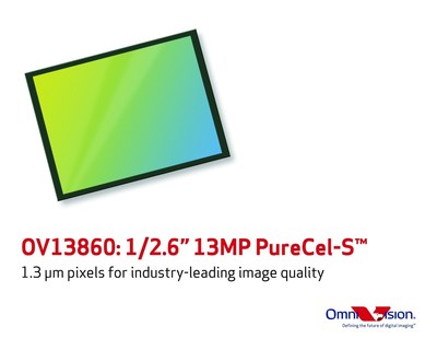
PureCel-S™ OV13860 with 35 Percent Larger Pixels Provides Best-in-Class Performance in Optimized Form Factor
SANTA CLARA, Calif., Oct. 6, 2014 — (PRNewswire) — OmniVision Technologies, Inc. (NASDAQ: OVTI), a leading developer of advanced digital imaging solutions, today announced the OV13860, a new 13-megapixel camera solution that brings best-in-class image quality to the next generation of premium smartphones. The 1/2.6-inch PureCel-S™ OV13860 image sensor uses large 1.3-micron pixels and leverages OmniVision's new stacked die technology to deliver exceptional low-light performance while meeting the design constraints of low z-height camera modules.
"Today's smartphone OEMs are conscious of the fact that users expect higher resolution cameras in their smartphones. But this increase in resolution is often accomplished by a reduction of pixel sizes, which results in a loss of camera performance and low-light sensitivity," said Bahman Hadji, product marketing manager at OmniVision. "The OV13860 is the ideal solution to this dilemma: a unique 1/2.6-inch 13-megapixel sensor with 1.3-micron pixels – 35 percent larger in size than traditional 13-megapixel sensors. Despite its 1/2.6-inch optical format, the OV13860 uses a high chief ray angle (CRA) to enable a camera module z-height of 5.5 mm, suitable for today's slim smartphones. With its large pixels and high CRA, the OV13860 provides an extraordinary 'no-compromise' imaging solution for next-generation flagship smartphones."
The PureCel-S™ OV13860 is the first in OmniVision's family of high-performance backside-illuminated PureCel™ image sensors to leverage the company's stacked die technology, which separates the imaging array from the image sensor processing pipeline into a stacked die structure. This allows for additional functionality to be implemented on the sensor while providing for a much smaller footprint when compared with non-stacked sensors, thus enabling smaller module sizes for larger optical format sensors.
Among the OV13860's advanced features is autofocus contrast calculation at an extremely fast 120 frames per second (FPS) while imaging at full 13-megapixel resolution to enable a fast autofocus camera system. When paired with a high-speed actuator, the OV13860 can provide for nearly instant autofocus by delivering contrast statistics at up to four times faster than traditional single frame-based contrast calculations. The OV13860 also supports alternate row dual-exposure high dynamic range (HDR) timing mode for delivering HDR video in challenging lighting scenes.
The OV13860's large 1.3-micron pixels enable dramatically improved high- and low-light performance as a result of higher sensitivity, signal-to-noise ratio, and full-well capacity when compared to products of similar or higher resolution with 1.12-micron pixels. The OV13860 can capture full-resolution 13-megapixel still images at 30 FPS or record ultra-high resolution 4K2K video at 30 FPS, 1080p full HD at 60 FPS, or 720p HD at 120 FPS. Each video output format includes additional pixels to support electronic image stabilization (EIS).
The OV13860 is currently sampling and is expected to enter volume production in the fourth quarter of 2014.
About OmniVision
OmniVision Technologies (NASDAQ:
OVTI) is a leading developer of advanced digital imaging solutions. Its award-winning CMOS imaging technology enables superior image quality in many of today's consumer and commercial applications, including mobile phones, notebooks, tablets and webcams, digital still and video cameras, security and surveillance, entertainment devices, automotive and medical imaging systems. Find out more at
www.ovt.com.
Safe-Harbor Language
Certain statements in this press release, including statements regarding the expected benefits, performance, capabilities, and potential market appeal, as well as anticipated timing of mass production, of the OV13860 are forward-looking statements that are subject to risks and uncertainties. These risks and uncertainties, which could cause the forward-looking statements and OmniVision's results to differ materially, include, without limitation: potential errors, design flaws or other problems with OV13860, customer acceptance, demand, and other risks detailed from time to time in OmniVision's Securities and Exchange Commission filings and reports, including, but not limited to, OmniVision's annual report filed on Form 10-K and quarterly reports filed on Form 10-Q. OmniVision expressly disclaims any obligation to update information contained in any forward-looking statement.
OmniVision® and the OmniVision logo are registered trademarks of OmniVision Technologies, Inc. PureCel™, PureCel-S™ are trademarks of OmniVision Technologies, Inc. All other trademarks are the property of their respective owners.

Photo - http://photos.prnewswire.com/prnh/20141004/150317
Logo - http://photos.prnewswire.com/prnh/20131107/SF12520LOGO-b
SOURCE OmniVision Technologies, Inc.
| Contact: |
| OmniVision Technologies, Inc.
Media, Martijn Pierik, Impress Labs, 602.366.5599 Email Contact Company, Scott Foster, OmniVision Technologies, 408.567.3077 Email Contact Investor Relations, Arnab Chanda, OmniVision Technologies, 408.653.3144 Email Contact Web: http://www.ovt.com |


