|
[ Chapter start ] [ Previous page ] [ Next page ] 17.1 Global RoutingThe details of global routing differ slightly between cell-based ASICs, gate arrays, and FPGAs, but the principles are the same in each case. A global router does not make any connections, it just plans them. We typically global route the whole chip (or large pieces if it is a large chip) before detail routing the whole chip (or the pieces). There are two types of areas to global route: inside the flexible blocks and between blocks (the Viterbi decoder, although a cell-based ASIC, only involved the global routing of one large flexible block). 17.1.1 Goals and ObjectivesThe input to the global router is a floorplan that includes the locations of all the fixed and flexible blocks; the placement information for flexible blocks; and the locations of all the logic cells. The goal of global routing is to provide complete instructions to the detailed router on where to route every net. The objectives of global routing are one or more of the following:
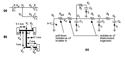
In both floorplanning and placement, with minimum interconnect length as an objective, it is necessary to find the shortest total path length connecting a set of terminals . This path is the MRST, which is hard to find. The alternative, for both floorplanning and placement, is to use simple approximations to the length of the MRST (usually the half-perimeter measure). Floorplanning and placement both assume that interconnect may be put anywhere on a rectangular grid, since at this point nets have not been assigned to the channels, but the global router must use the wiring channels and find the actual path. Often the global router needs to find a path that minimizes the delay between two terminals—this is not necessarily the same as finding the shortest total path length for a set of terminals. 17.1.2 Measurement of Interconnect DelayFloorplanning and placement need a fast and easy way to estimate the interconnect delay in order to evaluate each trial placement; often this is a predefined look-up table. After placement, the logic cell positions are fixed and the global router can afford to use better estimates of the interconnect delay. To illustrate one method, we shall use the Elmore constant to estimate the interconnect delay for the circuit shown in Figure 17.3 . The problem is to find the voltages at the inputs to logic cells B and C taking into account the parasitic resistance and capacitance of the metal interconnect. Figure 17.3 (c) models logic cell A as an ideal switch with a pull-down resistance equal to R pd and models the metal interconnect using resistors and capacitors for each segment of the interconnect. The Elmore constant for node 4 (labeled V 4 ) in the network shown in Figure 17.3 (c) is In Eq. 17.2 notice that R 24 = R pd + R 1 (and not R pd + R 1 + R 2 ) because R 1 is the resistance to V 0 (ground) shared by node 2 and node 4. Suppose we have the following parameters (from the generic 0.5 m m CMOS process, G5) for the layout shown in Figure 17.3 (b):
First we need to find the pull-down resistance, R pd , of the 4X inverter. If we model the gate with a linear pull-down resistor, R pd , driving a load C L , the output waveform is exp – t /( C L R pd ) (normalized to 1V). The output reaches 63 percent of its final value when t = C L R pd , because exp (–1) = 0.63. Then, because the delay is measured with a 0.65 trip point, the constant 0.5 nspF –1 = 0.5 k W is very close to the equivalent pull-down resistance. Thus, R pd ª 500 W . From the given data, we can calculate the R ’s and C ’s: Now we can calculate the path resistance, R ki , values (notice that R ki = R ik ): Finally, we can calculate Elmore’s constants for node 4 and node 2 as follows:
| ||||||||||||||||||||||||||||||||||||||||||||||||||||||||||||||||||||||||||||||||||||||||||||||||||||||||||||||||||||||||||||||||||||||||||||||||||||||||||||||||||||||||||||||||||||||||||||||||||||||||||||||||||||||||||||||||||||||||||||||||||


