16.3 Physical Design Flow
16.3 Physical
Design Flow
Historically placement was included with routing as a single tool (the term
P&R
is often used for place and route). Because interconnect delay now dominates gate delay, the trend is to include placement within a floorplanning tool and use a separate router.
Figure 16.31
shows a
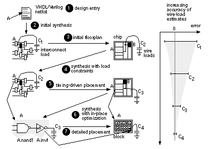
design flow using synthesis and a floorplanning tool that includes placement. This flow consists of the following steps:
-
Design entry.
The input is a logical description with no physical information.
-
Synthesis.
The initial synthesis contains little or no information on any interconnect loading. The output of the synthesis tool (typically an EDIF netlist) is the input to the floorplanner.
-
Initial floorplan.
From the initial floorplan interblock capacitances are input to the synthesis tool as load constraints and intrablock capacitances are input as wire-load tables.
-
Synthesis with load constraints.
At this point the synthesis tool is able to resynthesize the logic based on estimates of the interconnect capacitance each gate is driving. The synthesis tool produces a forward annotation file to constrain path delays in the placement step.
|

|
|
FIGURE 16.31
Timing-driven floorplanning and placement design flow. Compare with Figure 15.1 on p. 806.
|
-
Timing-driven placement.
After placement using constraints from the synthesis tool, the location of every logic cell on the chip is fixed and accurate estimates of interconnect delay can be passed back to the synthesis tool.
-
Synthesis
with
in-place optimization
(
IPO
). The synthesis tool changes the drive strength of gates based on the accurate interconnect delay estimates from the floorplanner without altering the netlist structure.
-
Detailed placement.
The placement information is ready to be input to the routing step.
In
Figure 16.31
we iterate between floorplanning and synthesis, continuously improving our estimate for the interconnect delay as we do so.
[ Chapter start ] [ Previous page ] [ Next page ] | 


