|
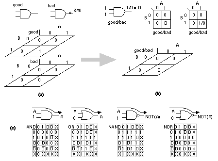
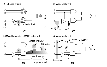
[ Chapter start ] [ Previous page ] [ Next page ] 14.5 Automatic Test-Pattern GenerationIn this section we shall describe a widely used algorithm, PODEM, for automatic test-pattern generation ( ATPG ) or automatic test-vector generation ( ATVG ). Before we can explain the PODEM algorithm we need to develop a shorthand notation and explain some terms and definitions using a simpler ATPG algorithm. 14.5.1 The D-CalculusFigure 14.17 (a) and (b) shows a shorthand notation, the D-calculus , for tracing faults. The D-calculus was developed by Roth [ 1966] together with an ATPG algorithm, the D-algorithm . The symbol D (for detect) indicates the value of a node is a logic '0' in the good circuit and a logic '1' in the bad circuit. We can also write this as D = 0/1. In general we write g/b, a composite logic value , to indicate a node value in the good circuit is g and b in the bad circuit (by convention we always write the good circuit value first and the faulty circuit value second). The complement of D is D = 1/0 ( D is rarely written as D' since D is a logic value just like '1' and '0'). Notice that D does not mean not detected, but simply that we see a '0' in the good circuit and a '1' in the bad circuit. We can apply Boolean algebra to the composite logic values D and D as shown in Figure 14.17 (c). The composite values 1/1 and 0/0 are equivalent to '1' and '0' respectively. We use the unknown logic value 'X' to represent a logic value that is one of '0', '1', D, or D , but we do not know or care which. If we wish to propagate a signal from one or more inputs of a logic cell to the logic cell output, we set the remaining inputs of that logic cell to what we call the enabling value . The enabling value is '1' for AND and NAND gates and '0' for OR and NOR gates. Figure 14.17 (c) illustrates the use of enabling values. In contrast, setting at least one input of a logic gate to the controlling value , the opposite of the enabling value for that gate, forces or justifies the output node of that logic gate to a fixed value. The controlling value of '0' for an AND gate justifies the output to '0' and for a NAND gate justifies the output to '1'. The controlling values of '1' justifies the output of an OR gate to '1' and justifies the output of a NOR gate to '0'. To find controlling and enabling values for more complex logic cells, such as AOI and OAI logic cells, we can use their simpler AND, OR, NAND, and NOR gate representations. 14.5.2 A Basic ATPG AlgorithmA basic algorithm to generate test vectors automatically is shown in Figure 14.18 . We detect a fault by first activating (or exciting the fault). To do this we must drive the faulty node to the opposite value of the fault. Figure 14.18 (a) shows a stuck-at-1 fault at the output pin, ZN, of the inverter U2 (we call this fault U2.ZN.SA1). To create a test for U2.ZN.SA1 we have to find the values of the PIs that will justify node U2.ZN to '0' . We work backward from node U2.ZN justifying each logic gate output until we reach a PI. In this case we only have to justify U2.ZN to '0' , and this is easily done by setting the PI A = '0'. Next we work forward from the fault origin and sensitize a path to a PO (there is only one PO in this example). This propagates the fault effect to the PO so that it may be observed . To propagate the fault effect to the PO Z, we set U3.A2 = '1' and then U5.A2 = '1'. We can visualize fault propagation by supposing that we set all nodes in a circuit to unknown, 'X'. Then, as we successively propagate the fault effect toward the POs, we can imagine a wave of D’s and D ’s, called the D-frontier , that propagates from the fault origin toward the POs. As a value of D or D reaches the inputs of a logic cell whose other inputs are 'X', we add that logic cell to the D-frontier. Then we find values for the other inputs to propagate the D-frontier through the logic cell to continue the process. This basic algorithm of justifying and then propagating a fault works when we can justify nodes without interference from other nodes. This algorithm breaks down when we have reconvergent fanout . Figure 14.19 (a) shows another example of justifying and propagating a fault in a circuit with reconvergent fanout. For direct comparison Figure 14.19 (b) shows an irredundant circuit, similar to part (a), except the fault signal, B stuck at 1, branches and then reconverges at the inputs to gate U5. The reconvergent fanout in this new circuit breaks our basic algorithm. We now have two sensitized paths that propagate the fault effect to U5. These paths combine to produce a constant '1' at Z, the PO. We have a multipath sensitization problem.
14.5.3 The PODEM AlgorithmThe path-oriented decision making ( PODEM ) algorithm solves the problem of reconvergent fanout and allows multipath sensitization [ Goel, 1981]. The method is similar to the basic algorithm we have already described except PODEM will retry a step, reversing an incorrect decision. There are four basic steps that we label: objective , backtrace , implication , and D-frontier . These steps are as follows:
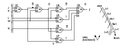
Figure 14.20 shows an example that uses the following iterations of the four steps in the PODEM algorithm:
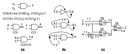
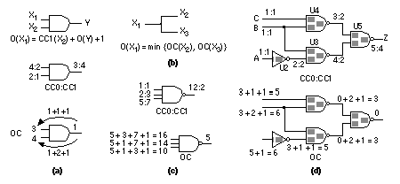
We can see that the PODEM algorithm proceeds in two phases. In the first phase, iterations 1 and 2 in Figure 14.20 , the objective is fixed in order to activate the fault. In the second phase, iterations 3–5, the objective changes in order to propagate the fault. In step 3 of the PODEM algorithm there must be at least one path containing unknown values between the gates of the D-frontier and a PO in order to be able to complete a sensitized path to a PO. This is called the X-path check . You may wonder why there has been no explanation of the backtrace mechanism or how to decide a value for a PI in step 2 of the PODEM algorithm. The decision tree shown in Figure 14.20 shows that it does not matter. PODEM conducts an implicit binary search over all the PIs. If we make an incorrect decision and assign the wrong value to a PI at some step, we will simply need to retry that step. Texts, programs, and articles use the term backtrace as we have described it, but then most use the term backtrack to describe what we have called a retry, which can be confusing. I also did not explain how to choose the objective in step 1 of the PODEM algorithm. The initial objective is to activate the fault. Subsequently we select a logic gate from the D-frontier and set one of its inputs to the enabling value in an attempt to propagate the fault. We can use intelligent procedures, based on controllability and observability , to guide PODEM and reduce the number of incorrect decisions. PODEM is a development of the D-algorithm, and there are several other ATPG algorithms that are developments of PODEM. One of these is FAN ( fanout-oriented test generation ) that removes the need to backtrace all the way to a PI, reducing the search time [ Fujiwara and Shimono, 1983; Schulz, Trischler, and Sarfert, 1988]. Algorithms based on the D-algorithm, PODEM, and FAN are the basis of many commercial ATPG systems. 14.5.4 Controllability and ObservabilityIn order for an ATPG system to provide a test for a fault on a node it must be possible to both control and observe the behavior of the node. There are both theoretical and practical issues involved in making sure that a design does not contain buried circuits that are impossible to observe and control. A software program that measures the controllability (with three l’ s) and observability of nodes in a circuit is useful in conjunction with ATPG software. There are several different measures for controllability and observability [ Butler and Mercer, 1992]. We shall describe one of the first such systems called SCOAP ( Sandia Controllability/Observability Analysis Program ) [ Goldstein, 1979]. These measures are also used by ATPG algorithms. Combinational controllability is defined separately from sequential controllability . We also separate zero-controllability and one-controllability . For example, the combinational zero-controllability for a two-input AND gate, Y = AND (X 1 , X 2 ), is recursively defined in terms of the input controllability values as follows: We choose the minimum value of the two-input controllability values to reflect the fact that we can justify the output of an AND gate to '0' by setting any input to the control value of '0'. We then add one to this value to reflect the fact that we have passed through an additional level of logic. Incrementing the controllability measures for each level of logic represents a measure of the logic distance between two nodes. We define the combinational one-controllability for a two-input AND gate as This equation reflects the fact that we need to set all inputs of an AND gate to the enabling value of '1' to justify a '1' at the output. Figure 14.21 (a) illustrates these definitions. An inverter, Y = NOT (X), reverses the controllability values: Since we can construct all other logic cells from combinations of two-input AND gates and inverters we can use Eqs. 14.5 – 14.7 to derive their controllability equations. When we do this we only increment the controllability by one for each primitive gate. Thus for a three-input NAND with an inverting input, Y = NAND (X 1 , X 2 , NOT (X 3 )): For a two-input NOR, Y = NOR (X 1 , X 2 ) = NOT (AND (NOT (X 1 ), NOT (X 2 )): Figure 14.21 (b) shows examples of controllability calculations. A bubble on a logic gate at the input or output swaps the values of CC1 and CC0. Figure 14.21 (c) shows how controllability values for a combinational circuit are calculated by working forward from each PI that is defined to have a controllability of one. We define observability in terms of the controllability measures. The combinational observability , OC (X 1 ), of input X 1 of a two-input AND gate can be expressed in terms of the controllability of the other input CC1 (X 2 ) and the combinational observability of the output, OC (Y): If a node X 1 branches (has fanout) to nodes X 2 and X 3 we choose the most observable of the branches: Figure 14.22 (a) and (b) show the definitions of observability. Figure 14.22 (c) illustrates calculation of observability at a three-input NAND; notice we sum the CC1 values for the other inputs (since the enabling value for a NAND gate is one, the same as for an AND gate). Figure 14.22 (d) shows the calculation of observability working back from the PO which, by definition, has an observability of zero. Sequential controllability and observability can be measured using similar equations to the combinational measures except that in the sequential measures (SC1, SC0, and OS) we measure logic distance in terms of the layers of sequential logic, not the layers of combinational logic. [ Chapter start ] [ Previous page ] [ Next page ] | ||||||||||||||||||||||||||||||||||||||||||||||||||||||||||||||||||||||

