|
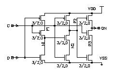
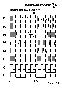
[ Chapter start ] [ Previous page ] [ Next page ] 13.9 Switch-Level SimulationThe switch-level simulator is a more detailed level of simulation than we have discussed so far. Figure 13.1 shows the circuit schematic of a true single-phase flip-flop using true single-phase clocking ( TSPC ). TSPC has been used in some full-custom ICs to attempt to save area and power. In a CMOS logic cell every node is driven to a strong '1' or a strong '0' . This is not true in TSPC, some nodes are left floating, so we ask the switch-level simulator to model charge leakage or charge decay (normally we need not worry about this low-level device issue). Figure 13.1 shows the waveform results. After five clock cycles, or 100 ns, we set the charge decay time to 5 ns. We notice two things. First, some of the node waveforms have values that are between logic '0' and '1' . Second, there are shaded areas on some node waveforms that represent the fact that, during the period of time marked, the logic value of the node is unknown. We can see that initially, before t = 100 ns (while we neglect the effects of charge decay), the circuit functions as a flip-flop. After t = 100 ns (when we begin including the effects of charge decay), the simulator tells us that this circuit may not function correctly. It is unlikely that all the charge would leak from a node in 5 ns, but we could not stop the clock in a design that uses a TSPC flip-flop. In ASIC design we do not use dangerous techniques such as TSPC and therefore do not normally need to use switch-level simulation. A switch-level simulator keeps track of voltage levels as well as logic levels, and it may do this in several ways. The simulator may use a large possible set of discrete values or the value of a node may be allowed to vary continuously. [ Chapter start ] [ Previous page ] [ Next page ] | |


