12.2  A Comparator/MUX

With the Verilog behavioral model of Figure 12.1 as the input, logic-synthesis software generates logic that performs the same function as the Verilog. The software then optimizes the logic to produce a structural model, which references logic cells from the cell library and details their connections.


`timescale 1ns / 10ps

module comp_mux_u (a, b, outp);

input [2:0] a; input [2:0] b;

output [2:0] outp;

supply1 VDD; supply0 VSS;


in01d0 u2 (.I(b[1]), .ZN(u2_ZN));

nd02d0 u3 (.A1(a[1]), .A2(u2_ZN), .ZN(u3_ZN));

in01d0 u4 (.I(a[1]), .ZN(u4_ZN));

nd02d0 u5 (.A1(u4_ZN), .A2(b[1]), .ZN(u5_ZN));

in01d0 u6 (.I(a[0]), .ZN(u6_ZN));

nd02d0 u7 (.A1(u6_ZN), .A2(u3_ZN), .ZN(u7_ZN));

nd02d0 u8 (.A1(b[0]), .A2(u3_ZN), .ZN(u8_ZN));

nd03d0 u9 (.A1(u5_ZN), .A2(u7_ZN), .A3(u8_ZN), .ZN(u9_ZN));

in01d0 u10 (.I(a[2]), .ZN(u10_ZN));

nd02d0 u11 (.A1(u10_ZN), .A2(u9_ZN), .ZN(u11_ZN));

nd02d0 u12 (.A1(b[2]), .A2(u9_ZN), .ZN(u12_ZN));

nd02d0 u13 (.A1(u10_ZN), .A2(b[2]), .ZN(u13_ZN));

nd03d0 u14 (.A1(u11_ZN), .A2(u12_ZN), .A3(u13_ZN), .ZN(u14_ZN));

nd02d0 u15 (.A1(a[2]), .A2(u14_ZN), .ZN(u15_ZN));

in01d0 u16 (.I(u14_ZN), .ZN(u16_ZN));

nd02d0 u17 (.A1(b[2]), .A2(u16_ZN), .ZN(u17_ZN));

nd02d0 u18 (.A1(u15_ZN), .A2(u17_ZN), .ZN(outp[2]));

nd02d0 u19 (.A1(a[1]), .A2(u14_ZN), .ZN(u19_ZN));

nd02d0 u20 (.A1(b[1]), .A2(u16_ZN), .ZN(u20_ZN));

nd02d0 u21 (.A1(u19_ZN), .A2(u20_ZN), .ZN(outp[1]));

nd02d0 u22 (.A1(a[0]), .A2(u14_ZN), .ZN(u22_ZN));

nd02d0 u23 (.A1(b[0]), .A2(u16_ZN), .ZN(u23_ZN));

nd02d0 u24 (.A1(u22_ZN), .A2(u23_ZN), .ZN(outp[0]));


endmodule


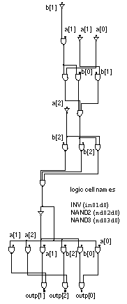
FIGURE 12.2  The comparator/MUX after logic synthesis, but before logic optimization. This figure shows the structural netlist, comp_mux_u.v , and its derived schematic.


`timescale 1ns / 10ps

module comp_mux_o (a, b, outp);

input [2:0] a; input [2:0] b;

output [2:0] outp;

supply1 VDD; supply0 VSS;


in01d0 B1_i1 (.I(a[2]), .ZN(B1_i1_ZN));

in01d0 B1_i2 (.I(b[1]), .ZN(B1_i2_ZN));

oa01d1 B1_i3 (.A1(a[0]), .A2(B1_i4_ZN), .B1(B1_i2_ZN), .B2(a[1]), .ZN(B1_i3_Z;

fn05d1 B1_i4 (.A1(a[1]), .B1(b[1]), .ZN(B1_i4_ZN));

fn02d1 B1_i5 (.A(B1_i3_ZN), .B(B1_i1_ZN), .C(b[2]), .ZN(B1_i5_ZN));

mx21d1 B1_i6 (.I0(a[0]), .I1(b[0]), .S(B1_i5_ZN), .Z(outp[0]));

mx21d1 B1_i7 (.I0(a[1]), .I1(b[1]), .S(B1_i5_ZN), .Z(outp[1]));

mx21d1 B1_i8 (.I0(a[2]), .I1(b[2]), .S(B1_i5_ZN), .Z(outp[2]));


endmodule


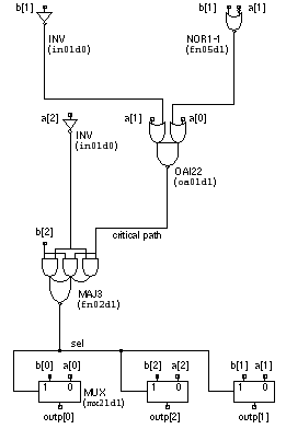
FIGURE 12.3  The comparator/MUX after logic synthesis and logic optimization with the default settings. This figure shows the structural netlist, comp_mux_o.v , and its derived schematic.

Before running a logic synthesizer, it is necessary to set up paths and startup files ( synopsys_dc.setup , compass.boo , view.ini , or similar). These files set the target library and directory locations. Normally it is easier to run logic synthesis in text mode using a script. A script is a text file that directs a software tool to execute a series of synthesis commands (we call this a synthesis run ). Figure 12.2 shows a structural netlist, comp_mux_u.v , and the derived schematic after logic synthesis, but before any logic optimization . A derived schematic is created by software from a structural netlist (as opposed to a schematic drawn by hand).
shows the structural netlist, comp_mux_o.v , and the derived schematic after logic optimization is performed (with the default settings). Figures 12.2 and 12.3 show the results of the two separate steps: logic synthesis and logic optimization. Confusingly, the whole process, which includes synthesis and optimization (and other steps as well), is referred to as logic synthesis . We also refer to the software that performs all of these steps (even if the software consists of more than one program) as a logic synthesizer .

Logic synthesis parses (in a process sometimes called analysis ) and translates (sometimes called elaboration ) the input HDL to a data structure. This data structure is then converted to a network of generic logic cells. For example, the network in Figure 12.2 uses NAND gates (each with three or fewer inputs in this case) and inverters. This network of generic logic cells is technology-independent since cell libraries in any technology normally contain NAND gates and inverters. The next step, logic optimization , attempts to improve this technology-independent network under the controls of the designer. The output of the optimization step is an optimized, but still technology-independent, network. Finally, in the logic-mapping step, the synthesizer maps the optimized logic to a specified technology-dependent target cell library. Figure 12.3 shows the results of using a standard-cell library as the target.

Text reports such as the one shown in Table 12.3 may be the only output that the designer sees from the logic-synthesis tool. Often, synthesized ASIC netlists and the derived schematics containing thousands of logic cells are far too large to follow. To make things even more difficult, the net names and instance names in synthesized netlists are automatically generated. This makes it hard to see which lines of code in the HDL generated which logic cells in the synthesized netlist or derived schematic.

TABLE 12.3  Reports from the logic synthesizer for the Verilog version of the comparator/MUX.

Command

Synthesizer output 1

> synthesize

                 Num Gate Count Tot Gate Width Total

Cell Name Insts Per Cell Count Per Cell Width

--------- ----- ---------- -------- -------- --------

in01d0 5 .8 3.8 7.2 36.0

nd02d0 16 1.0 16.0 9.6 153.6

nd03d0 2 1.3 2.5 12.0 24.0

--------- ----- ---------- -------- -------- --------

Totals: 23 22.2 213.6


> optimize

                 Num Gate Count Tot Gate Width Total

Cell Name Insts Per Cell Count Per Cell Width

--------- ----- ---------- -------- -------- --------

fn02d1 1 1.8 1.8 16.8 16.8

fn05d1 1 1.3 1.3 12.0 12.0

in01d0 2 .8 1.5 7.2 14.4

mx21d1 3 2.2 6.8 21.6 64.8

oa01d1 1 1.5 1.5 14.4 14.4

--------- ----- ---------- -------- -------- --------

Totals: 8 12.8 122.4


> report timing

instance name

inPin --> outPin incr arrival trs rampDel cap cell

                      (ns) (ns) (ns) (pf)

----------------------------------------------------------------------

a[1] .00 .00 R .00 .04 comp_m...

B1_i4

A1 --> ZN .33 .33 R .17 .03 fn05d1

B1_i3

A2 --> ZN .39 .72 F .33 .06 oa01d1

B1_i5

A --> ZN 1.03 1.75 R .67 .11 fn02d1

B1_i6

S --> Z .68 2.43 R .09 .02 mx21d1


In the comparator/MUX example the derived schematics are simple enough that, with hindsight, it is clear that the XOR logic cell used in the hand design is logically inefficient. Using XOR logic cells does, however, result in the simple schematic of Figure 12.1 . The synthesized version of the comparator/MUX in Figure 12.3 uses complex combinational logic cells that are logically efficient, but the schematic is not as easy to read. Of course, the computer does not care about this—and neither do we since we usually never see the schematic.

Which version is best—the hand-designed or the synthesized version? Table 12.3 shows statistics generated by the logic synthesizer for the comparator/MUX. To calculate the performance of each circuit that it evaluates during synthesis, there is a timing-analysis tool (also known as a timing engine ) built into the logic synthesizer. The timing-analysis tool reports that the critical path in the optimized comparator/MUX is 2.43 ns. This critical path is highlighted on the derived schematic of Figure 12.3 and consists of the following delays:

  • 0.33 ns due to cell fn05d1 , instance name B1_i4 , a two-input NOR cell with an inverted input. We might call this a NOR1-1 or (A + B')' logic cell.
  • 0.39 ns due to cell oa01d1 , instance name B1_i3 , an OAI22 logic cell.
  • 1.03 ns due to logic cell fn02d1 , instance name B1_i5 , a three-input majority function, MAJ3 (A, B, C).
  • 0.68 ns due to logic cell mx21d1 , instance name B1_i6 , a 2:1 MUX.

(In this cell library the 'd1' suffix indicates normal drive strength.)

TABLE 12.4  Logic cell comparisons between the two comparator/MUX designs.

Cell type

Library cell name 2

3 tPLH /ns

tPHL /ns

Gate equivalents in cell 4

Cells used in hand

design

Cells used in

synthesized design

Gate equivalents used

by hand design

Gate equivalents used in

synthesized design

Width of cell 5 / m m

Width used by

hand design / m m

Width of synthesized

design / m m

Inverter

in01d0

0.37

0.36

0.8

2

2

1.6

1.6

7.2

14.4

14.4

2-input XOR

xo02d1

0.93

0.62

1.8

3

5.3

16.8

50.4

2-input AND

an02d1

0.34

0.46

1.3

1

1.3

12.0

12.0

3-input AND

an03d1

0.38

0.52

1.5

1

1.5

14.4

14.4

4-input AND

an04d1

0.41

0.98

1.8

1

1.8

16.8

16.8

3-input OR

or03d1

0.60

0.44

1.8

1

1.8

16.8

16.8

2-input MUX

mx21d1

0.69

0.68

2.2

3

3

6.6

6.6

21.6

64.8

64.8

AOI22

oa01d1

0.51

0.42

1.5

1

1.5

14.4

14.4

MAJ3

fn02d1

0.84

0.81

1.8

1

1.8

16.8

16.8

NOR1-1= (A' + B)'

fn05d1 6

0.42

0.46

1.3

1

1.3

12.0

12.0

Totals


12

8

19.8

12.8


189.6

122.4

Table 12.4 lists the name, type, the number of transistors, the area, and the delay of each logic cell used in the hand-designed and synthesized comparator/MUX. We could have performed this analysis by hand using the cell-library data book and a calculator or spreadsheet, but it would have been tedious work—especially calculating the delays. The computer is excellent at this type of bookkeeping. We can think of the timing engine of a logic synthesizer as a logic calculator.

We see from Table 12.4 that the sum of the widths of all the cells used in the synthesized design (122.4 m m) is less than for the hand design (189.6 m m). All the standard cells in a library are the same height, 72 l or 21.6 m m, in this case. Thus the synthesized design is smaller. We could estimate the critical path of the hand design using the information from the cell-library data book (summarized in Table 12.4 ). Instead we will use the timing engine in the logic synthesizer as a logic calculator to extract the critical path for the hand-designed comparator/MUX.

Table 12.5 shows a timing analysis obtained by loading the hand-designed schematic netlist into the logic synthesizer. Table 12.5 shows that the hand-designed (critical path 2.42 ns) and synthesized versions (critical path 2.43 ns) of the comparator/MUX are approximately the same speed. Remember, though, that we used the default settings during logic optimization. Section 12.11 shows that the logic synthesizer can do much better.

TABLE 12.5  Timing report for the hand-designed version of the comparator/MUX using the logic
synthesizer to calculate the critical path (compare with Table 12.3 ).

Command

Synthesizer output 7

> report timing

instance name

inPin --> outPin incr arrival trs rampDel cap cell

                      (ns) (ns) (ns) (pf)

----------------------------------------------------------------------

a[1]                    .00      .00    F    .00     .04    comp_mux

B1_i4

A1 --> ZN               .61      .61    F    .14     .03    xo02d1

B1_i3

A2 --> ZN               .85     1.46    F    .19     .05    an04d1

B1_i5

A --> ZN                .42     1.88    F    .23     .09    or03d1

B1_i6

S --> Z                 .54     2.42    R    .09     .02    mx21d1

outp[0]                 .00     2.42    R    .00     .00    comp_mux

12.2.1 An Actel Version of the Comparator/MUX

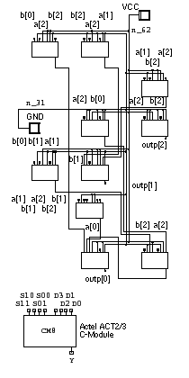
Figure 12.4 shows the results of targeting the comparator/MUX design to the Actel ACT 2/3 FPGA architecture. (The EDIF converter prefixes all internal nodes in this netlist with 'block_0_DEF_NET_' . This prefix was replaced with 'n_' in the Verilog file, comp_mux_actel_o_adl_e.v , derived from the .adl netlist.) As can be seen by comparing the netlists and schematics in Figures  12.3 and 12.4 , the results are very different between a standard-cell library and the Actel library. Each of the symbols in the schematic in Figure 12.4 represents the eight-input ACT 2/3 C-Module (see Figure 5.4 a). The logic synthesizer, during the technology-mapping step, has decided which connections should be made to the inputs to the combinational logic macro, CM8 . The CM8 names and the ACT2/3 C-Module names (in parentheses) correspond as follows: S00(A0) , S01(B0) , S10(A1) , S11(A2) , D0(D00) , D1(D01) , D2(D10) , D3(D11) , and Y(Y) .

`timescale 1 ns/100 ps

module comp_mux_actel_o (a, b, outp);

input [2:0] a, b; output [2:0] outp;

wire n_13, n_17, n_19, n_21, n_23, n_27, n_29, n_31, n_62;


CM8 I_5_CM8(.D0(n_31), .D1(n_62), .D2(a[0]), .D3(n_62), .S00(n_62), .S01(n_13), .S10(n_23), .S11(n_21), .Y(outp[0]));

CM8 I_2_CM8(.D0(n_31), .D1(n_19), .D2(n_62), .D3(n_62), .S00(n_62), .S01(b[1]), .S10(n_31), .S11(n_17), .Y(outp[1]));

CM8 I_1_CM8(.D0(n_31), .D1(n_31), .D2(b[2]), .D3(n_31), .S00(n_62), .S01(n_31), .S10(n_31), .S11(a[2]), .Y(outp[2]));

VCC VCC_I(.Y(n_62));

CM8 I_4_CM8(.D0(a[2]), .D1(n_31), .D2(n_62), .D3(n_62), .S00(n_62), .S01(b[2]), .S10(n_31), .S11(a[1]), .Y(n_19));

CM8 I_7_CM8(.D0(b[1]), .D1(b[2]), .D2(n_31), .D3(n_31), .S00(a[2]), .S01(b[1]), .S10(n_31), .S11(a[1]), .Y(n_23));

CM8 I_9_CM8(.D0(n_31), .D1(n_31), .D2(a[1]), .D3(n_31), .S00(n_62), .S01(b[1]), .S10(n_31), .S11(b[0]), .Y(n_27));

CM8 I_8_CM8(.D0(n_29), .D1(n_62), .D2(n_31), .D3(a[2]), .S00(n_62), .S01(n_27), .S10(n_31), .S11(b[2]), .Y(n_13));

CM8 I_3_CM8(.D0(n_31), .D1(n_31), .D2(a[1]), .D3(n_31), .S00(n_62), .S01(a[2]), .S10(n_31), .S11(b[2]), .Y(n_17));

CM8 I_6_CM8(.D0(b[2]), .D1(n_31), .D2(n_62), .D3(n_62), .S00(n_62), .S01(a[2]), .S10(n_31), .S11(b[0]), .Y(n_21));

CM8 I_10_CM8(.D0(n_31), .D1(n_31), .D2(b[0]), .D3(n_31), .S00(n_62), .S01(n_31), .S10(n_31), .S11(a[2]), .Y(n_29));

GND GND_I(.Y(n_31));

endmodule


FIGURE 12.4  The Actel version of the comparator/MUX after logic optimization. This figure shows the s tructural netlist, comp_mux_actel_o_adl_e.v , and its derived schematic.


1. Cell Name  = cell name from the ASIC library (Compass Passport, 0.6 m m high-density, 5 V standard-cell library, cb60hd230); Num Insts  = number of cell instances; Gate Count Per Cell = equivalent gates with two-input NAND = 1 gate (with number of transistors ª equivalent gates  ¥  4); Width Per Cell = width in m m (cell height in this library is 72 l or 21.6 m m); incr  = incremental delay time due to logic cell delay; trs  = transition; R  = rising; F  = falling; rampDel  = ramp delay; cap  = capacitance at node or cell output pin.

2. 0.6 m m, 5 V, high-density Compass standard-cell library, cb60hd230.

3. Average over all inputs with load capacitance equal to two standard loads (one standard load = 0.016 pF).

4. 2-input NAND = 1 gate equivalent.

5. Cell height is 72 l (21.6 m m).

6. Rise and fall delays are different for the two inputs, A and B, of this cell: t PLHA = 0.48 ns; t PLHB = 0.36 ns; t PHLA = 0.59 ns; t PHLB = 0.33 ns.

7. See footnote 1 in Table 12.3 for explanations of the abbreviations used in this table.


Chapter start ] [ Previous page ] [ Next page ]


© 2025 Internet Business Systems, Inc.
670 Aberdeen Way, Milpitas, CA 95035
+1 (408) 882-6554 — Contact Us, or visit our other sites:
AECCafe - Architectural Design and Engineering TechJobsCafe - Technical Jobs and Resumes GISCafe - Geographical Information Services  MCADCafe - Mechanical Design and Engineering ShareCG - Share Computer Graphic (CG) Animation, 3D Art and 3D Models
  Privacy PolicyAdvertise