|
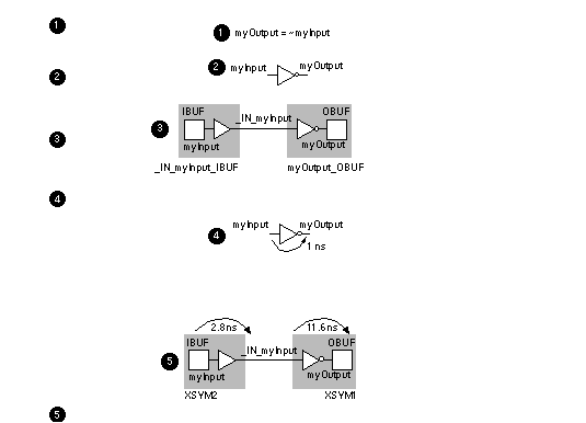
[ Chapter start ] [ Previous page ] [ Next page ] 8.3 The Halfgate ASICThis section illustrates FPGA design using a very simple ASIC—a single inverter. The hidden details of the design and construction of this “halfgate FPGA” are quite complicated. Fortunately, most of the inner workings of the design software are normally hidden from the designer. However, when software breaks, as it sometimes does, it is important to know how things work in order to fix the problem. The formats, filenames, and flow will change, but the information needed at each stage and the order in which it is conveyed will stay much the same. 8.3.1 XilinxTable 8.5 shows an FPGA design flow using Compass and Xilinx software. On the left of Table 8.5 is a script for the Compass programs—scripts for Cadence, Mentor, and Synopsys software are similar, but not all design software has the capability to be run on autopilot using scripts and a command language. The diagrams in Table 8.5 illustrate what is happening at each of the design steps. The following numbered comments, corresponding to the labels in Table 8.5 , highlight the important steps:
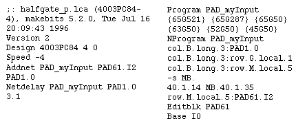
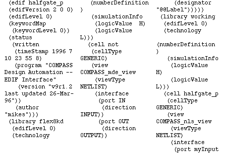
Table 8.6 shows the key Xilinx files that are created. The preroute file, halfgate_p.xnf , describes the IBUF and OBUF library cells but does not contain any delays. The LCA file, halfgate_p.lca , contains all the physical design information, including the locations of the pads and I/O cells on the FPGA ( PAD61 for myInput and PAD1 for myOutput ), as well as the details of the programmable connections between these I/O Cells. The postroute file, halfgate_b.xnf , is similar to the preroute version except that now the delays are included. Xilinx assigns delays to a pin (connector or terminal of a cell). In this case 2.8 ns is assigned to the output of the input buffer, 8.6 ns is assigned to the input of the output buffer, and finally 3.0 ns is assigned to the output of the output buffer. 8.3.2 ActelThe key Actel files for the halfgate design are the netlist file, halfgate_io.adl, and the STF delay file for back-annotation, halfgate_io.stf. Both of these files are shown in Table 8.7 (the STF file is large and only the last few lines, which contain the delay information, are shown in the table). 8.3.3 AlteraBecause Altera complex PLDs use a deterministic routing structure, they can be designed more easily using a self-contained software package—an “all-in-one” software package using a single interface. We shall assume that we can generate a netlist that the Altera software can accept using Cadence, Mentor, or Compass software with an Altera design kit (the most convenient format is EDIF). Table 8.8 shows the EDIF preroute netlist in a format that the Altera software can accept. This netlist file describes a single inverter (the line 'cellRef not'). The majority of the EDIF code in Table 8.8 is a standard template to pass information about how the VDD and VSS nodes are named, which libraries are used, the name of the design, and so on. We shall cover EDIF in Chapter 9 .
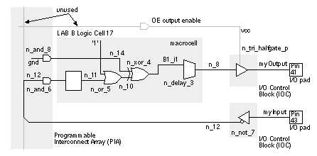
Table 8.9 shows a small part of the reports generated by the Altera software after completion of the place-and-route step. This report tells us how the software has used the basic logic cells, interconnect, and I/O cells to implement our design. With practice it is possible to read the information from reports such as Table 8.9 directly, but it is a little easier if we also look at the netlist. The EDIF version of postroute netlist for this example is large. Fortunately, the Altera software can also generate a Verilog version of the postroute netlist. Here is the generated Verilog postroute netlist, halfgate_p.vo (not '.v' ), for the halfgate design: // halfgate_p (EPM7032LC44) MAX+plus II Version 5.1 RC6 10/03/94 module TRI_halfgate_p( IN, OE, OUT ); input IN; input OE; output OUT; specparam TTRI = 40; specparam TTXZ = 60; specparam TTZX = 60; (OE => OUT) = (0,0, TTXZ, TTZX, TTXZ, TTZX); module halfgate_p (myInput, myOutput); input myInput; output myOutput; supply0 gnd; supply1 vcc; wire B1_i1, myInput, myOutput, N_8, N_10, N_11, N_12, N_14; TRI_halfgate_p tri_2 ( .OUT(myOutput), .IN(N_8), .OE(vcc) ); TRANSPORT transport_3 ( N_8, N_8_A ); defparam transport_3.DELAY = 10; xor xor2_4 ( B1_i1, N_10, N_14 ); TRANSPORT transport_6 ( N_11, N_11_A ); defparam transport_6.DELAY = 60; TRANSPORT transport_7 ( N_12, N_12_A ); defparam transport_7.DELAY = 40; not not_7 ( N_12_A, myInput ); TRANSPORT transport_8 ( N_14, N_14_A ); defparam transport_8.DELAY = 60; The Verilog model for our ASIC, halfgate_p , is written in terms of other models: and , xor , or , not , TRI_halfgate_p , TRANSPORT . The first four of these are primitive models for basic logic cells and are built into the Verilog simulator. The model for TRI_halfgate_p is generated together with the rest of the code. We also need the following model for TRANSPORT, which contains the delay information for the Altera MAX complex PLD. This code is part of a file ( alt_max2.vo ) that is generated automatically. // MAX+plus II Version 5.1 RC6 10/03/94 Wed Jul 17 04:07:10 1996 module TRANSPORT( OUT, IN ); input IN; output OUT; reg OUTR; wire OUT = OUTR; parameter DELAY = 0; The Altera software can also write the following VHDL postroute netlist: -- halfgate_p (EPM7032LC44) MAX+plus II Version 5.1 RC6 10/03/94 LIBRARY IEEE; USE IEEE.std_logic_1164.all; GENERIC (ttri: TIME := 1 ns; ttxz: TIME := 1 ns; ttzx: TIME := 1 ns); PORT (in0 : IN X01Z; oe : IN X01Z; out0: OUT X01Z); ARCHITECTURE behavior OF n_tri_halfgate_p IS IF oe = '0' THEN out0 <= TRANSPORT 'Z' AFTER ttxz; ELSIF oe = '1' THEN out0 <= TRANSPORT in0 AFTER ttzx; ELSIF oe = '1' THEN out0 <= TRANSPORT in0 AFTER ttri; LIBRARY IEEE; USE IEEE.std_logic_1164.all; USE work.n_tri_halfgate_p; PORT ( myInput : IN X01Z; myOutput : OUT X01Z); ARCHITECTURE EPM7032LC44 OF n_halfgate_p IS SIGNAL gnd : X01Z := '0'; SIGNAL vcc : X01Z := '1'; SIGNAL n_8, B1_i1, n_10, n_11, n_12, n_14 : X01Z; GENERIC (ttri, ttxz, ttzx: TIME); PORT (in0, oe : IN X01Z; out0 : OUT X01Z); PROCESS(myInput) BEGIN ASSERT myInput /= 'X' OR Now = 0 ns REPORT "Unknown value on myInput" SEVERITY Warning; GENERIC MAP (ttri => 4 ns, ttxz => 6 ns, ttzx => 6 ns) PORT MAP (in0 => n_8, oe => vcc, out0 => myOutput); n_delay_3: n_8 <= TRANSPORT B1_i1 AFTER 1 ns; n_xor_4: B1_i1 <= n_10 XOR n_14; n_and_6: n_11 <= TRANSPORT n_12 AFTER 6 ns; n_not_7: n_12 <= TRANSPORT NOT myInput AFTER 4 ns; n_and_8: n_14 <= TRANSPORT gnd AFTER 6 ns; LIBRARY IEEE; USE IEEE.std_logic_1164.all; USE work.n_halfgate_p; PORT ( myInput : IN std_logic; myOutput : OUT std_logic); ARCHITECTURE EPM7032LC44 OF halfgate_p IS COMPONENT n_halfgate_p PORT (myInput : IN X01Z; myOutput : OUT X01Z); PORT MAP ( myInput => TO_X01Z(myInput), myOutput => myOutput); The VHDL is a little harder to decipher than the Verilog, so the schematic for the VHDL postroute netlist is shown in Figure 8.2 . This VHDL netlist is identical in function to the Verilog netlist, but the net names and component names are different. Compare Figure 8.2 with Figure 5.15 (c) in Section 5.4 , “ Altera MAX ,” which shows the Altera basic logic cell and Figure 6.23 in Section 6.8, “Other I/O Cells,” which describes the Altera I/O cell. The software has fixed the inputs to the various elements in the Altera MAX device to implement a single inverter.
8.3.4 ComparisonThe halfgate ASIC design illustrates the differences between a nondeterministic coarse-grained FPGA (Xilinx XC4000), a nondeterministic fine-grained FPGA (Actel ACT 3), and a deterministic complex PLD (Altera MAX 7000). These differences, summarized as follows, were apparent even in the halfgate design:
[ Chapter start ] [ Previous page ] [ Next page ] | |||||||||


