|
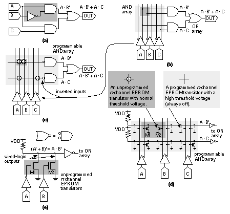
[ Chapter start ] [ Previous page ] [ Next page ] 5.4 Altera MAXSuppose we have a simple two-level logic circuit that implements a sum of products as shown in Figure 5.11 (a). We may redraw any two-level circuit using a regular structure ( Figure 5.11 b): a vector of buffers, followed by a vector of AND gates (which construct the product terms) that feed OR gates (which form the sums of the product terms). We can simplify this representation still further ( Figure 5.11 c), by drawing the input lines to a multiple-input AND gate as if they were one horizontal wire, which we call a product-term line . A structure such as Figure 5.11 (c) is called programmable array logic , first introduced by Monolithic Memories as the PAL series of devices.
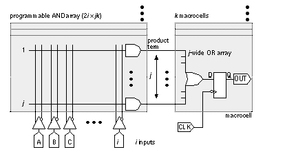
Because the arrangement of Figure 5.11 (c) is very similar to a ROM, we sometimes call a horizontal product-term line, which would be the bit output from a ROM, the bit line . The vertical input line is the word line . Figure 5.11 (d) and (e) show how to build the programmable-AND array (or product-term array) from EPROM transistors. The horizontal product-term lines connect to the vertical input lines using the EPROM transistors as pull-downs at each possible connection. Applying a '1' to the gate of an unprogrammed EPROM transistor pulls the product-term line low to a '0'. A programmed n -channel transistor has a threshold voltage higher than V DD and is therefore always off . Thus a programmed transistor has no effect on the product-term line. Notice that connecting the n -channel EPROM transistors to a pull-up resistor as shown in Figure 5.11 (e) produces a wired-logic function—the output is high only if all of the outputs are high, resulting in a wired-AND function of the outputs. The product-term line is low when any of the inputs are high. Thus, to convert the wired-logic array into a programmable-AND array, we need to invert the sense of the inputs. We often conveniently omit these details when we draw the schematics of logic arrays, usually implemented as NOR–NOR arrays (so we need to invert the outputs as well). They are not minor details when you implement the layout, however. Figure 5.12 shows how a programmable-AND array can be combined with other logic into a macrocell that contains a flip-flop. For example, the widely used 22V10 PLD, also called a registered PAL, essentially contains 10 of the macrocells shown in Figure 5.12 . The part number, 22V10, denotes that there are 22 inputs (44 vertical input lines for both true and complement forms of the inputs) to the programmable AND array and 10 macrocells. The PLD or registered PAL shown in Figure 5.12 has an 2 i ¥ jk programmable-AND array.
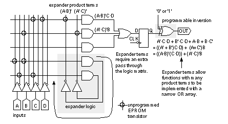
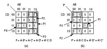
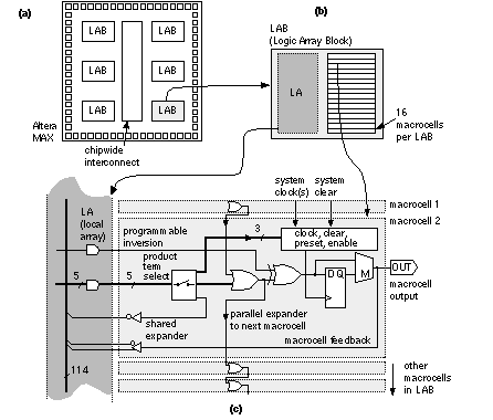
5.4.1 Logic ExpandersThe basic logic cell for the Altera MAX architecture, a macrocell, is a descendant of the PAL. Using the logic expander , shown in Figure 5.13 to generate extra logic terms, it is possible to implement functions that require more product terms than are available in a simple PAL macrocell. As an example, consider the following function: F = A' · C · D + B' · C · D + A · B + B · C'.(5.22) This function has four product terms and thus we cannot implement F using a macrocell that has only a three-wide OR array (such as the one shown in Figure 5.13 ). If we rewrite F as a “sum of (products of products)” like this: F = (A' + B') · C · D + (A + C') · B = (A · B)' (C · D) + (A' · C)' · B ;(5.23) we can use logic expanders to form the expander terms (A · B)' and (A' · C)' (see Figure 5.13 ). We can even share these extra product terms with other macrocells if we need to. We call the extra logic gates that form these shareable product terms a shared logic expander , or just shared expander . The disadvantage of the shared expanders is the extra logic delay incurred because of the second pass that you need to take through the product-term array. We usually do not know before the logic tools assign logic to macrocells ( logic assignment ) whether we need to use the logic expanders. Since we cannot predict the exact timing the Altera MAX architecture is not strictly deterministic . However, once we do know whether a signal has to go through the array once or twice, we can simply and accurately predict the delay. This is a very important and useful feature of the Altera MAX architecture. The expander terms are sometimes called helper terms when you use a PAL. If you use helper terms in a 22V10, for example, you have to go out to the chip I/O pad and then back into the programmable array again, using two-pass logic . Another common feature in complex PLDs, also used in some PLDs, is shown in Figure 5.13 . Programming one input of the XOR gate at the macrocell output allows you to choose whether or not to invert the output (a '1' for inversion or to a '0' for no inversion). This programmable inversion can reduce the required number of product terms by using a de Morgan equivalent representation instead of a conventional sum-of-products form, as shown in Figure 5.14 . As an example of using programmable inversion, consider the function F = A · B' + A · C' + A · D' + A' · C · D ,(5.24) which requires four product terms—one too many for a three-wide OR array. If we generate the complement of F instead, F ' = A · B · C · D + A' · D' + A' · C' ,(5.25) this has only three product terms. To create F we invert F ', using programmable inversion. Figure 5.15 shows an Altera MAX macrocell and illustrates the architectures of several different product families. The implementation details vary among the families, but the basic features: wide programmable-AND array, narrow fixed-OR array, logic expanders, and programmable inversion—are very similar. 1 Each family has the following individual characteristics:
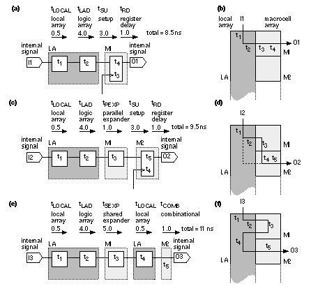
5.4.2 Timing ModelFigure 5.16 shows the Altera MAX timing model for local signals. 2 For example, in Figure 5.16 (a) an internal signal, I1, enters the local array (the LAB interconnect with a fixed delay t 1 = t LOCAL = 0.5 ns), passes through the AND array (delay t 2 = t LAD = 4.0 ns), and to the macrocell flip-flop (with setup time, t 3 = t SU = 3.0 ns, and clock–Q or register delay , t 4 = t RD = 1.0 ns). The path delay is thus: 0.5 + 4 +3 + 1 = 8.5 ns. Figure 5.16 (c) illustrates the use of a parallel logic expander . This is different from the case of the shared expander ( Figure 5.13 ), which required two passes in series through the product-term array. Using a parallel logic expander, the extra product term is generated in an adjacent macrocell in parallel with other product terms (not in series—as in a shared expander). We can illustrate the difference between a parallel expander and a shared expander using an example function that we have used before (Eq. 5.22 ), F = A' · C · D + B' · C · D + A · B + B · C' .(5.26) This time we shall use macrocell M1 in Figure 5.16 (d) to implement F1 equal to the sum of the first three product terms in Eq. 5.26 . We use F1 (using the parallel expander connection between adjacent macrocells shown in Figure 5.15 ) as an input to macrocell M2. Now we can form F = F1 + B · C' without using more than three inputs of an OR gate (the MAX 5000 has a three-wide OR array in the macrocell, the MAX 9000, as shown in Figure 5.15 , is capable of handling five product terms in one macrocell—but the principle is the same). The total delay is the same as before, except that we add the delay of a parallel expander, t PEXP = 1.0 ns. Total delay is then 8.5 + 1 = 9.5 ns. Figure 5.16 (e) and (f) shows the use of a shared expander—similar to Figure 5.13 . The Altera MAX macrocell is more like a PLD than the other FPGA architectures discussed here; that is why Altera calls the MAX architecture a complex PLD. This means that the MAX architecture works well in applications for which PLDs are most useful: simple, fast logic with many inputs or variables. 5.4.3 Power Dissipation in Complex PLDsA programmable-AND array in any PLD built using EPROM or EEPROM transistors uses a passive pull-up (a resistor or current source), and these macrocells consume static power . Altera uses a switch called the Turbo Bit to control the current in the programmable-AND array in each macrocell. For the MAX 7000, static current varies between 1.4 mA and 2.2 mA per macrocell in high-power mode (the current depends on the part—generally, but not always, the larger 7000 parts have lower operating currents) and between 0.6 mA and 0.8 mA in low-power mode. For the MAX 9000, the static current is 0.6 mA per macrocell in high-current mode and 0.3 mA in low-power mode, independent of the part size. 3 Since there are 16 macrocells in a LAB and up to 35 LABs on the largest MAX 9000 chip (16 ¥ 35 = 560 macrocells), just the static power dissipation in low-power mode can be substantial (560 ¥ 0.3 mA ¥ 5 V = 840 mW). If all the macrocells are in high-power mode, the static power will double. This is the price you pay for having an (up to) 114-wide AND gate delay of a few nanoseconds (t LAD = 4.0 ns) in the MAX 9000. For any MAX 9000 macrocell in the low-power mode it is necessary to add a delay of between 15 ns and 20 ns to any signal path through the local interconnect and logic array (including t LAD and t PEXP ). [ Chapter start ] [ Previous page ] [ Next page ] | ||||

