|
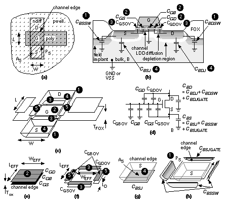
[ Chapter start ] [ Previous page ] [ Next page ] 3.2 Transistor Parasitic CapacitanceLogic-cell delay results from transistor resistance, transistor (intrinsic) parasitic capacitance, and load (extrinsic) capacitance. When one logic cell drives another, the parasitic input capacitance of the driven cell becomes the load capacitance of the driving cell and this will determine the delay of the driving cell. Figure 3.4 shows the components of transistor parasitic capacitance. SPICE prints all of the MOS parameter values for each transistor at the DC operating point. The following values were printed by PSpice (v5.4) for the simulation of Figure 3.3 :
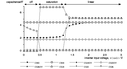
NAME m1 m2 The parameters ID ( I DS ), VGS , VDS , VBS , VTH (V t ), and VDSAT (V DS (sat) ) are DC parameters. The parameters GM , GDS , and GMB are small-signal conductances (corresponding to ∂ I DS /∂ V GS , ∂ I DS /∂ V DS , and ∂ I DS /∂ V BS , respectively). The remaining parameters are the parasitic capacitances. Table 3.1 shows the calculation of these capacitance values for the n -channel transistor m1 (with W = 6 m m and L = 0.6 m m) in Figure 3.3 (a). 3.2.1 Junction CapacitanceThe junction capacitances, C BD and C BS , consist of two parts: junction area and sidewall; both have different physical characteristics with parameters: CJ and MJ for the junction, CJSW and MJSW for the sidewall, and PB is common. These capacitances depend on the voltage across the junction ( V DB and V SB ). The calculations in Table 3.1 assume both source and drain regions are 6 m m ¥ 1.2 m m rectangles, so that A D = A S = 7.2 ( m m) 2 , and the perimeters (excluding the 1.2 m m channel edge) are P D = P S = 6 + 1.2 + 1.2 = 8.4 m m. We exclude the channel edge because the sidewalls facing the channel (corresponding to C BSJ GATE and C BDJ GATE in Figure 3.4 ) are different from the sidewalls that face the field. There is no standard method to allow for this. It is a mistake to exclude the gate edge assuming it is accounted for in the rest of the model—it is not. A pessimistic simulation includes the channel edge in P D and P S (but a true worst-case analysis would use more accurate models and worst-case model parameters). In HSPICE there is a separate mechanism to account for the channel edge capacitance (using parameters ACM and CJGATE ). In Table 3.1 we have neglected C J GATE . For the p -channel transistor m2 (W = 12 m m and L = 0.6 m m) the source and drain regions are 12 m m ¥ 1.2 m m rectangles, so that A D = A S ª 14 ( m m) 2 , and the perimeters are P D = P S = 12 + 1.2 + 1.2 ª 14 m m (these parameters are rounded to two significant figures solely to simplify the figures and tables). In passing, notice that a 1.2 m m strip of diffusion in a 0.6 m m process ( l = 0.3 m m) is only 4 l wide—wide enough to place a contact only with aggressive spacing rules. The conservative rules in Figure 2.11 would require a diffusion width of at least 2 (rule 6.4a) + 2 (rule 6.3a) + 1.5 (rule 6.2a) = 5.5 l . 3.2.2 Overlap CapacitanceThe overlap capacitance calculations for C GSOV and C GDOV in Table 3.1 account for lateral diffusion (the amount the source and drain extend under the gate) using SPICE parameter LD = 5E-08 or L D = 0.05 m m. Not all versions of SPICE use the equivalent parameter for width reduction, WD (assumed zero in Table 3.1 ), in calculating C GDOV and not all versions subtract W D to form W EFF . 3.2.3 Gate CapacitanceThe gate capacitance calculations in Table 3.1 depend on the operating region. The gate–source capacitance C GS varies from zero when the transistor is off to 0.5C O (0.5 ¥ 1.035 ¥ 10 –15 = 5.18 ¥ 10 –16 F) in the linear region to (2/3)C O in the saturation region (6.9 ¥ 10 –16 F). The gate–drain capacitance C GD varies from zero (off) to 0.5C O (linear region) and back to zero (saturation region). The gate–bulk capacitance C GB may be viewed as two capacitors in series: the fixed gate-oxide capacitance, C O = W EFF L EFF e ox / T ox , and the variable depletion capacitance, C S = W EFF L EFF e Si / x d , formed by the depletion region that extends under the gate (with varying depth x d ). As the transistor turns on the conducting channel appears and shields the bulk from the gate—and at this point C GB falls to zero. Even with V GS = 0 V, the depletion width under the gate is finite and thus C GB ª 4 ¥ 10 –15 F is less than C O ª 10 –16 F. In fact, since C GB ª 0.5 C O , we can tell that at V GS = 0 V, C S ª C O . Figure 3.5 shows the variation of the parasitic capacitance values.
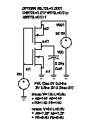
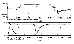
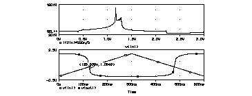
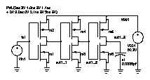
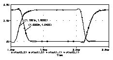
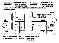
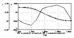
3.2.4 Input Slew RateFigure 3.6 shows an experiment to monitor the input capacitance of an inverter as it switches. We have introduced another variable—the delay of the input ramp or the slew rate of the input. In Figure 3.6 (b) the input ramp is 40 ps long with a slew rate of 3 V/ 40 ps or 75 GVs –1 —as in our previous experiments—and the output of the inverter hardly moves before the input has changed. The input capacitance varies from 20 to 40 fF with an average value of approximately 34 fF for both transitions—we can measure the average value in Probe by plotting AVG(-i(Vin)) . In Figure 3.6 (c) the input ramp is slow enough (300 ns) that we are switching under almost equilibrium conditions—at each voltage we allow the output to find its level on the static transfer curve of Figure 3.2 (a). The switching waveforms are quite different. The average input capacitance is now approximately 0.04 pF (a 20 percent difference). The propagation delay (using an input trip point of 0.5 and an output trip point of 0.35) is negative and approximately 150 – 127 = –23 ns. By changing the input slew rate we have broken our model. For the moment we shall ignore this problem and proceed. The calculations in Table 3.1 and behavior of Figures 3.5 and 3.6 are very complex. How can we find the value of the parasitic capacitance, C , to fit the model of Figure 3.1 ? Once again, as we did for pull resistance and the intrinsic output capacitance, instead of trying to derive a theoretical value for C, we adjust the value to fit the model. Before we formulate another experiment we should bear in mind the following questions that the experiment of Figure 3.6 raises: Is it valid to replace the nonlinear input capacitance with a linear component? Is it valid to use a linear input ramp when the normal waveforms are so nonlinear? Figure 3.7 shows an experiment crafted to answer these questions. The experiment has the following two steps:
We can summarize our findings from this and previous experiments as follows:
The last two observations are useful. Since the gate capacitances are nonlinear, we only see about 0.025/0.037 or 70 percent of the 0.037 pF gate-oxide capacitance, C O , in the input capacitance, C . This means that it happens by chance that the total gate-oxide capacitance is also a rough estimate of the gate input capacitance, C ª C O . Using L and W rather than L EFF and W EFF in Eq. 3.9 helps this estimate. The accuracy of this estimate depends on the fact that the junction capacitances are approximately one-third of the gate-oxide capacitance—which happens to be true for many CMOS processes for the shapes of transistors that normally occur in logic cells. In the next section we shall use this estimate to help us design logic cells. [ Chapter start ] [ Previous page ] [ Next page ] | ||||||||||

