|
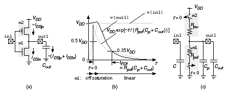
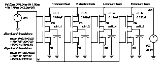
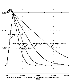
[ Chapter start ] [ Previous page ] [ Next page ] 3.1 Transistors as ResistorsIn Section 2.1, “CMOS Transistors,” we modeled transistors using ideal switches. If this model were accurate, logic cells would have no delay. The ramp input, v(in1) , to the inverter in Figure 3.1 (a) rises quickly from zero to V DD . In response the output, v(out1) , falls from V DD to zero. In Figure 3.1 (b) we measure the propagation delay of the inverter, t PD , using an input trip point of 0.5 and output trip points of 0.35 (falling, t PDf ) and 0.65 (rising, t PDr ). Initially the n -channel transistor, m1 , is off . As the input rises, m1 turns on in the saturation region ( V DS > V GS – V t n ) before entering the linear region ( V DS < V GS – V t n ). We model transistor m1 with a resistor, R pd (Figure 3.1 c); this is the pull-down resistance . The equivalent resistance of m2 is the pull-up resistance , R pu . Delay is created by the pull-up and pull-down resistances, R pd and R pu , together with the parasitic capacitance at the output of the cell, C p (the intrinsic output capacitance ) and the load capacitance (or extrinsic output capacitance ), C out (Figure 3.1 c). If we assume a constant value for R pd , the output reaches a lower trip point of 0.35 when (Figure 3.1 b), An output trip point of 0.35 is convenient because ln (1/0.35) = 1.04 ª 1 and thus
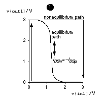
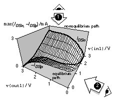
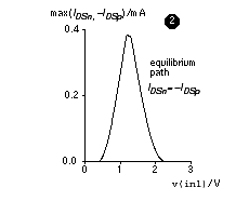
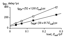
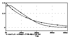
The expression for the rising delay (with a 0.65 output trip point) is identical in form. Delay thus increases linearly with the load capacitance. We often measure load capacitance in terms of a standard load —the input capacitance presented by a particular cell (often an inverter or two-input NAND cell). We may adjust the delay for different trip points. For example, for output trip points of 0.1/0.9 we multiply Eq. 3.2 by –ln(0.1) = 2.3, because exp (–2.3) = 0.100. Figure 3.2 shows the DC characteristics of a CMOS inverter. To form Figure 3.2 (b) we take the n -channel transistor surface (Figure 2.4b) and add that for a p -channel transistor (rotated to account for the connections). Seen from above, the intersection of the two surfaces is the static transfer curve of Figure 3.2 (a)—along this path the transistor currents are equal and there is no output current to change the output voltage. Seen from one side, the intersection is the curve of Figure 3.2 (c). The input waveform, v(in1) , and the output load (which determines the transistor currents) dictate the path we take on the surface of Figure 3.2 (b) as the inverter switches. We can thus see that the currents through the transistors (and thus the pull-up and pull-down resistance values) will vary in a nonlinear way during switching. Deriving theoretical values for the pull-up and pull-down resistance values is difficult—instead we work the problem backward by picking the trip points, simulating the propagation delays, and then calculating resistance values that fit the model. Figure 3.3 shows a simulation experiment (using the G5 process SPICE parameters from Table 2.1). From the results in Figure 3.3 (c) we can see that R pd = 817 W and R pu = 1281 W for this inverter (with shape factors of 6/0.6 for the n -channel transistor and 12/0.6 for the p -channel) using 0.5 (input) and 0.35/0.65 (output) trip points. Changing the trip points would give different resistance values. We can check that 817 W is a reasonable value for the pull-down resistance. In the saturation region I DS (sat) is (to first order) independent of V DS . For an n -channel transistor from our generic 0.5 m m process (G5 from Section 2.1) with shape factor W/L = 6/0.6, I DSn (sat) = 2.5 mA (at V GS = 3V and V DS = 3V). The pull-down resistance, R 1 , that would give the same drain–source current is This value is greater than, but not too different from, our measured pull-down resistance of 817 W . We might expect this result since Figure 3.2b shows that the pull-down resistance reaches its maximum value at V GS = 3V, V DS = 3V. We could adjust the ratio of the logic so that the rising and falling delays were equal; then R = R pd = R pu is the pull resistance . Next, we check our model against the simulation results. The model predicts ( t' is measured from the point at which the input crosses the 0.5 trip point, t' = 0 at t = 20 ps). With C p = 4 standard loads = 4 ¥ 0.034 pF = 0.136 pF, To make a comparison with the simulation we need to use ln (1/0.35) = 1.04 and not approximately 1 as we have assumed, so that (with all times in ps) Equation 3.6 is plotted in Figure 3.3 (d). For v(out1) = 1.05 V (equal to the 0.35 output trip point), Eq. 3.6 predicts t = 20 + 149.112 ª 169 ps and agrees with Figure 3.3 (b)—it should because we derived the model from these results! Now we find C p . From Figure 3.3 (c) and Eq. 3.2
These intrinsic parasitic capacitance values depend on the choice of output trip points, even though C pf R pdf and C pr R pdr are constant for a given input trip point and waveform, because the pull-up and pull-down resistances depend on the choice of output trip points. We take a closer look at parasitic capacitance next. [ Chapter start ] [ Previous page ] [ Next page ] | ||||||||||||||||||||||||||||||||||||||||||||||||||||||||||||||||||||||||||||||||||||

