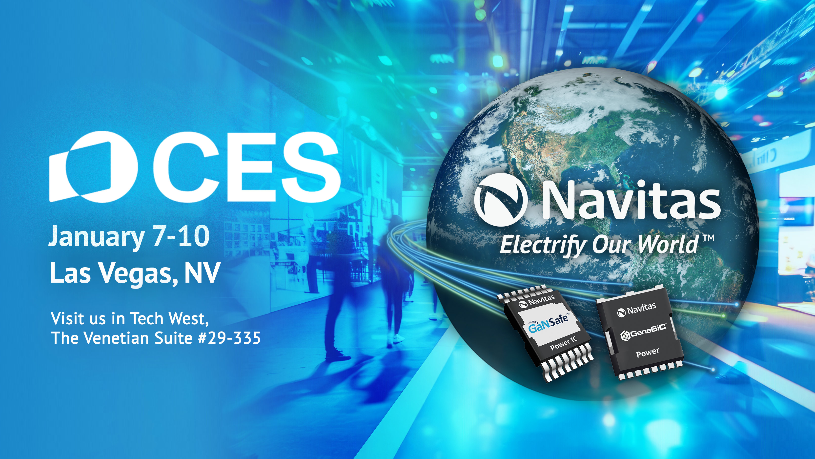
TORRANCE, Calif., Dec. 05, 2024 (GLOBE NEWSWIRE) -- Navitas Semiconductor (Nasdaq: NVTS), the only pure-play, next-generation power semiconductor company and industry leader in gallium nitride (GaN) power ICs and silicon carbide (SiC) technology, has announced it will showcase several breakthroughs for AI data centers, EVs, and mobile technology at CES 2025 (Tech West, Venetian suite 29-335, January 7th - 10th). Navitas was recently acknowledged as the Top 500 fastest-growing technology company, by Deloitte’s Technology Fast 500™, for the third consecutive year.

The “Planet Navitas” suite will showcase the company’s mission to ‘Electrify our World™’ by advancing the transition from legacy silicon to next-generation, clean energy, GaN and SiC power semiconductors. These technologies are designed for high growth markets that demand the highest efficiency and power density, such as AI data centers, electric vehicles (EVs), and mobile. Additionally, Navitas will demonstrate how GaN and SiC technologies contribute to reducing carbon-footprint, with the potential to save over 6,000 megatons of CO2 per year by 2050.
Major technology and system breakthroughs include:
- World’s only 650V bi-directional GaNFast™ power ICs: Game-changing, disruptive GaN technology for next-generation solutions that require the highest efficiency and power density, with the lowest complexity, and significant component reduction.
-
World’s First 8.5 kW AI Data Center Power Supply: See the world’s first 8.5 kW OCP power solution achieving 98% efficiency for AI and hyperscale data centers. Featuring high-power GaNSafe™ power ICs and Gen-3 Fast SiC MOSFETs in 3-Phase Interleaved CCM Totem-Pole PFC and 3-Phase LLC topologies to provide the highest efficiency, performance, and lowest component count.
-
World’s Highest Power Density AI Power Supply: Navitas delivers efficient 4.5 kW power in the smallest power-supply form-factor for the latest AI GPUs that demand 3x more power per rack. The optimized design uses high-power GaNSafe ICs and Gen-3 Fast SiC MOSFETs enabling the world’s highest power density with 137 W/in3 and over 97% efficiency.
- ‘
IntelliWeave’ Patented Digital Control Optimized for AI Data Center Power Supplies: Combined with high-power GaNSafe™ and Gen-3 ‘Fast’ SiC MOSFETs to enable PFC peak efficiencies of 99.3% and reduce power losses by 30% compared to existing solutions.
-
Automotive Qualified (AEC-Q101) Gen-3 Fast SiC MOSFETs with ‘trench-assisted planar’ technology: Enabled by over 20 years of SiC innovation leadership, GeneSiC™ technology leads on performance with the Gen-3 ‘Fast’ SiC MOSFETs with ‘trench-assisted planar’ technology. This proprietary technology provides world-leading performance over temperature, delivering cool-running, fast-switching, and superior robustness to support faster charging EVs and up to 3x more powerful AI data centers.
-
GaNSlim™: Simple. Fast. Integrated: A new generation of highly-integrated GaN power ICs that will further simplify and speed the development of small form factor, high-power-density applications by offering the highest level of integration and thermal performance. Target applications include chargers for mobile devices and laptops, TV power supplies, and lighting systems of up to 500W.
- SiCPAK™ High-Power Modules – Built for Endurance and Performance: Utilizing industry-leading 'trench-assisted planar'-gate technology and epoxy-resin potting for increased power cycling and long-lasting reliability, SiCPAK modules offer compact form factors and provide cost-effective, power-dense solutions for applications including EV charging, drives, solar, and energy storage systems (ESS).
- New Advancements in our Leading GaNFast & GeneSiC technology:
- GaNSense™ motor drive ICs with bi-directional loss-less current sensing, voltage sensing, and temperature protection, further enhancing performance and robustness beyond what is achievable by any discrete GaN or discrete silicon device.
- GeneSiC MOSFET die specifically optimized for EV traction modules with additional screening and gold metallization for sintering.
- Sustainable Solutions: Discover Navitas' vision to reduce up to 6 Gtons/year of CO₂ by 2050 with technologies that offer higher efficiency, density, and grid independence.
CES 2025 takes place in Las Vegas, NV from January 7th – 10th. The “Planet Navitas” suite is located in Tech West at the Venetian, suite 29-335.
To schedule a press meeting with Navitas at CES, please
book here (via Calendly)
To schedule an IR meeting, please
book here.
About Navitas
Navitas Semiconductor (Nasdaq: NVTS) is the only pure-play, next-generation power-semiconductor company, celebrating
10 years of power innovation founded in 2014.
GaNFast™ power ICs integrate gallium nitride (GaN) power and drive, with control, sensing, and protection to enable faster charging, higher power density, and greater energy savings. Complementary
GeneSiC™ power devices are optimized high-power, high-voltage, and high-reliability silicon carbide (SiC) solutions. Focus markets include AI datacenters, EV, solar, energy storage, home appliance / industrial, mobile and consumer. Over 300 Navitas patents are issued or pending, with the industry’s first and only
20-year GaNFast warranty. Navitas was the world’s first semiconductor company to be
CarbonNeutral®-certified.
Navitas Semiconductor, GaNFast, GaNSense, GeneSiC and the Navitas logo are trademarks or registered trademarks of Navitas Semiconductor Limited and affiliates. All other brands, product names and marks are or may be trademarks or registered trademarks used to identify products or services of their respective owners.
Contact Information
Llew Vaughan-Edmunds, Sr Director, Product Management & Marketing
info@navitassemi.com
Stephen Oliver, VP Investor Relations
ir@navitassemi.com
A photo accompanying this announcement is available at https://www.globenewswire.com/NewsRoom/AttachmentNg/e3889989-7b5b-400d-a033-f2870c9cc9c4
