TORRANCE, Calif., Sept. 04, 2024 (GLOBE NEWSWIRE) --
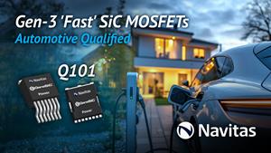
Navitas Semiconductor (Nasdaq: NVTS), the industry leader in next-generation GaNFast™ gallium nitride (GaN) and GeneSiC™ silicon carbide (SiC) power semiconductors, today announced the release of a portfolio of third-generation automotive-qualified SiC MOSFETs in D2PAK-7L (TO-263-7) and TOLL (TO-Leadless) surface-mount (SMT) packages.
Navitas’ proprietary ‘ trench-assisted planar’ technology provides world-leading performance over temperature and delivers high-speed, cool-running operation for electric vehicle (EV) charging, traction, and DC-DC conversion. With case temperatures up to 25°C lower than conventional devices, Gen-3 Fast SiC offers an operating life up to 3x longer than alternative SiC products, for high-stress EV environments.
Gen-3 Fast MOSFETs are optimized for the fastest switching speed, highest efficiency, and support increased power density in EV applications such as AC compressors, cabin heaters, DC-DC converters, and on-board chargers (OBCs). Navitas’ dedicated EV Design Center has demonstrated leading edge OBC system solutions up to 22 kW with 3.5 kW/liter power density, and over 95.5% efficiency.
400 V-rated EV battery architectures are served by the new 650 V Gen-3 Fast MOSFETs featuring RDS(ON) ratings from 20 to 55 mΩ. The 1,200 V ranges from 18 to 135 mΩ and is optimized for 800 V systems.
Both 650 and 1,200 V ranges are AEC Q101-qualified in the traditional SMT D2PAK-7L (TO-263-7) package. For 400 V EVs, the 650 V-rated, surface-mount TOLL package offers a 9% reduction in junction-to-case thermal resistance (RTH,J-C), 30% smaller PCB footprint, 50% lower height, and 60% smaller size than the D2PAK-7L. This enables very high-power density solutions, while minimal package inductance of only 2 nH ensures excellent fast-switching performance and lowest dynamic package losses.
The automotive-qualified 650 V and 1200 V G3F SiC MOSFET family in D2PAK-7L and TOLL surface mount packages are released and available immediately for purchase. For more information, please contact info@navitassemi.com.
About Navitas
Navitas Semiconductor (Nasdaq: NVTS) is the only pure-play, next-generation power-semiconductor company, celebrating 10 years of power innovation founded in 2014. GaNFast™ power ICs integrate gallium nitride (GaN) power and drive, with control, sensing, and protection to enable faster charging, higher power density, and greater energy savings. Complementary GeneSiC™ power devices are optimized high-power, high-voltage, and high-reliability silicon carbide (SiC) solutions. Focus markets include EV, solar, energy storage, home appliance / industrial, data center, mobile, and consumer. Over 250 Navitas patents are issued or pending. Navitas offers the industry’s first and only 20-year GaNFast warranty and was the world’s first semiconductor company to be CarbonNeutral®-certified.
Navitas Semiconductor, GaNFast, GaNSense, GeneSiC, and the Navitas logo are trademarks or registered trademarks of Navitas Semiconductor Limited and affiliates. All other brands, product names, and marks are or may be trademarks or registered trademarks used to identify products or services of their respective owners.
Contact Information:
Llew Vaughan-Edmunds, Sr Director, Product Management & Marketing
info@navitassemi.com
Stephen Oliver, VP Investor Relations
ir@navitassemi.com
A photo accompanying this announcement is available at https://www.globenewswire.com/NewsRoom/AttachmentNg/4f90db45-f60b-4e1b-ad90-0cf756d84ec6
