Highlights:
SUNNYVALE, Calif., June 17, 2020 — (PRNewswire) — Rambus Inc. (NASDAQ: RMBS), a premier silicon IP and chip provider making data faster and safer, today announced it has expanded its portfolio of high-speed interface IP on TSMC's industry-leading 7nm process with the addition of its silicon-demonstrated 112G XSR/USR PHY. Offering unmatched power and area efficiency for next-generation applications, the 112G XSR/USR PHY is a critical enabler of chiplet and CPO architectures for data center, networking, 5G, HPC and AI/ML applications."Chiplets are already entering mainstream markets to enable cost-effective, high-performance products and to maintain signal integrity across variable physical distances," said Shane Rau, research vice president, computing semiconductors at IDC. "SerDes PHYs at advanced process nodes, like the 7nm 112G XSR, enable that speed and signal integrity."
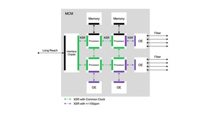
The accelerated trend of disaggregation of large SoCs into multiple smaller chiplets demands faster time to market, yield improvement and design flexibility. The Rambus 112G XSR/USR PHY is a critical enabler of the D2D and D2OE interconnects for chiplet architectures. Implemented on TSMC's advanced process technology, this chiplet connectivity solution has been demonstrated in silicon to exceed the challenging reach/BER performance of the CEI-112G XSR specification, and supports NRZ and PAM-4 signaling at various data rates for maximum design flexibility.
"We're pleased with the availability of Rambus' PHY on our N7 process technology to address the growing market need for low-power, high-performance chiplet architectures," said Suk Lee, senior director of the Design Infrastructure Management Division at TSMC. "Our ongoing partnership with Rambus ensures that designers can meet next-generation requirements for performance and power efficiency in computing, AI/ML and networking using TSMC's advanced process technologies."
Leading-edge applications moving to chiplet architectures include next-generation 51.2 Terabit per second (Tbps) ASICs for network switches, where 112G XSR links will connect the digital switch ASIC die to CPO engines. In AI/ML and HPC SoCs, the 112G XSR PHY can be used to bridge purpose-built accelerator chiplets for natural language processing, video transcoding and image recognition. Another popular use case is the die disaggregation of large SoCs, hitting reticle size limits for manufacturable yields, into multiple smaller die connected using XSR links over organic substrate. Increasingly, these advanced applications are implemented on TSMC's N7 process.
"This important milestone highlights Rambus' leadership in high-speed SerDes enabling the industry's highest value and most demanding applications," said Hemant Dhulla, vice president and general manager of IP cores at Rambus. "At an industry-leading power efficiency of sub-picojoule per bit, and unidirectional bandwidth approaching two terabit per second per millimeter, we are very proud to offer our 112G XSR/USR solution in partnership with TSMC."
Availability
The Rambus 112G XSR/USR PHY is available today for licensing and integrating into chiplet and SoC designs.
Additional Information
For additional details about the Rambus 112G XSR/USR PHY, please go to
https://www.rambus.com/interface-ip/serdes/112g-xsr-phy/
Follow Rambus:
Company website:
rambus.com
Rambus blog:
rambus.com/blog
Twitter:
@rambusinc
LinkedIn:
www.linkedin.com/company/rambus
Facebook:
www.facebook.com/RambusInc
About Rambus Inc.
Rambus is a premier silicon IP and chip provider that makes data faster and safer. With 30 years of innovation, we continue to develop the foundational technology for all modern computing systems. Leveraging our semiconductor expertise, Rambus solutions speed performance, expand capacity and improve security for today's most demanding applications. From data center and edge to artificial intelligence and automotive, our interface and security IP, and memory interface chips enable SoC and system designers to deliver their vision of the future. For more information, visit
rambus.com.
Press Contact:
Cori Pasinetti
Rambus Corporate Communications
t: (408) 462-8306
cpasinetti@rambus.com
![]() View original content to download multimedia:
http://www.prnewswire.com/news-releases/rambus-delivers-112g-xsrusr-phy-on-tsmc-7nm-process-for-chiplets-and-co-packaged-optics-in-networking-and-data-center-301079001.html
View original content to download multimedia:
http://www.prnewswire.com/news-releases/rambus-delivers-112g-xsrusr-phy-on-tsmc-7nm-process-for-chiplets-and-co-packaged-optics-in-networking-and-data-center-301079001.html
SOURCE Rambus Inc.
| Contact: |
| Company Name: Rambus Inc.
Web: www.rambus.com Financial data for Rambus Inc. |


