


TOKYO — (BUSINESS WIRE) — October 30, 2018 — Toshiba Electronic Devices & Storage Corporation (“Toshiba”) today announced the launch of "TCB702FNG," an addition to its 4-channel high-efficiency linear power amplifiers that meet current market requirements for high efficiency. Sample shipments start today with mass production scheduled to begin in the first quarter of 2019.
This press release features multimedia. View the full release here: https://www.businesswire.com/news/home/20181030006234/en/
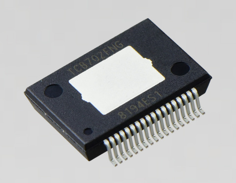
Toshiba: A 4-channel high-efficiency linear power amplifier "TCB702FNG" with 45W output. (Photo: Business Wire)
With "TCB702FNG," Toshiba has improved on its technology to realize efficiency comparable with a digital high efficiency of class D amplifier in actual operating range (0.5 to 4W). Power consumption is cut by up to 80% of that for a typical class AB amplifier[1]. The new IC’s maximum output is 45W, and the IC is pin-compatible with “TCB701FNG,” the company’s high efficiency linear power amplifier with maximum 50W output.
The new amplifier also includes a self-diagnosis function with I2C bus control that can diagnose errors and contribute to a suitable set design by changing the detection setting for gain or time constants. It also includes full-time error detection of output DC offset voltage, which can quickly detect abnormal output offset voltage and prevent speaker burnout, improving set reliability.
|
Main specifications |
||
| Part number | TCB702FNG | |
| Maximum output | 45W×4ch (Vcc=15.2V,RL=4Ω, MaxPower) | |
| Supply voltage | 6V to 18V | |
|
Total harmonic
|
0.02% (Pout=0.4W) | |
| Output noise voltage | 60μVrms (BW=DIN_AUDIO) | |
| Power consumption |
Up to 80% lower than a typical class AB amplifier
(supply voltage=14.4V in case of 0.8W output) |
|
|
Functions and
|
・ 6V operations ・ Full-time error detection for output DC offset voltage ・ I 2 C bus control allows diagnosis of errors such as cross output connection. ・ Various detections are selectable from two or more settings, such as a gain, mute time constants and temperature ・ Can be used as both a power amplifier and line output amplifier. ・ Various built-in protection circuits (output cross connection, over voltage, and low voltage) |
|
| Package | P-HSSOP36-1116-0.65-001 | |


 Animation, 3D Art and 3D Models")