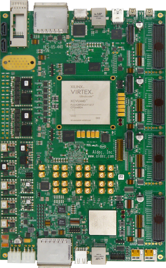
Henderson, Nev. – February 28, 2017 – Aldec, Inc., a pioneer in mixed HDL language simulation and hardware-assisted verification for ASIC and FPGA designs, unveils the latest HES™ prototyping board HES-US-440 along with a new release of HES-DVM™ software that enables Simulation Acceleration and Emulation modes for the HES-US-440 board in addition to Physical Prototyping.
The new HES-US-440 board joins Aldec’s growing portfolio of HES boards featuring Xilinx® UltraScale™ FPGA. It is targeted to physical prototyping of small to medium sized ASIC designs up to 26 Million gates and large FPGA designs. In addition to the main Virtex® UltraScale XCVU440 FPGA, the board contains the largest device Z100 of Xilinx Zynq®-7000 used as a host module, two independent DDR4 SO-DIMM ports supporting up to 64GB of DRAM memory, and four FMC HPC standardized connectors facilitating board extension with any kind of peripherals available on mezzanine daughter cards from Aldec or third party vendors.
Concurrently with the release of its latest board, Aldec has released a new version of HES-DVM 2017.02 software that enables Simulation Acceleration and Emulation modes for this new board. With the new release of HES-DVM, the HES-US-440 prototyping board can be used to accelerate HDL simulation with any kind of testbench including a transaction level UVM. The board can also be used to run hybrid co-emulation with virtual models. The transaction-level connection with HDL simulators or virtual platforms is based on Accellera’s SCE-MI standard and has been built upon the fast PCI Express x8 host interface.
 “After last year’s very successful launch of Aldec’s
HES-US-1320 board containing three Xilinx UltraScale XCVU440 FPGAs with a capacity of 79 million ASIC gates scalable up to 316 million with backplane, we received queries about a single FPGA UltraScale board that could be utilized as a versatile desktop prototyping platform to aid design verification with hardware-in-the-loop without the need of using partitioning tools,” said Zibi Zalewski, General Manager of Hardware Division. “This new HES-US-440 board is Aldec’s answer to this demand and its design is based on our customer’s feedback and ideas, one being the use of the Xilinx Zynq device as a host controller. It combines dual-core ARM® Cortex®-A9 with programmable FPGA logic, enabling users to create a self-contained, software-driven, embedded testbench running on an ARM module and generating AXI or AHB transactions to the design implemented in Virtex UltraScale FPGA. This is only one of many use cases and this board supported by the new HES-DVM software can be continually used throughout entire design verification.”
Availability
The new HES-US-440 and HES-DVM™ 2017.02 software are available now. To learn more or to evaluate visit www.aldec.com, e-mail Email Contact, call +1 (702) 990-4400, or contact our worldwide distribution partners.
About HES™ Prototyping
Aldec offers a portfolio of HES™ prototyping boards based on the largest Xilinx FPGA of the Virtex UltraScale and Virtex-7 families. The boards are architected to allow for easy expansion using BPX backplane and standardized FMC and BPX daughter card connectors.
About HES-DVM™
HES-DVM™ is a fully automated and scalable hybrid verification environment for SoC and ASIC designs. Utilizing the latest co-emulation standards like SCE-MI or TLM and the newest FPGA technology, hardware and software design teams obtain early access to the hardware prototype of the design. HES-DVM is used in labs worldwide for all kinds of emulation tasks including Simulation Acceleration, Hybrid Virtual Prototypes, In-Circuit Emulation, and Software Validation at MHz speeds. Learn more about Aldec Hardware Emulation Solutions.
About Aldec
Aldec Inc., headquartered in Henderson, Nevada, is an industry leader in Electronic Design Verification and offers a patented technology suite including: RTL Design, RTL Simulators, Hardware-Assisted Verification, SoC and ASIC Prototyping, Design Rule Checking, CDC Verification, IP Cores, Requirements Lifecycle Management, DO-254 Functional Verification, Embedded Solutions and Military/Aerospace solutions. http://www.aldec.com/
Contact:
Christina Toole, Aldec, Inc.
+ (702) 990-4400
Email Contact