SAN JOSE, Calif. — (BUSINESS WIRE) — November 11, 2014 — Checkpoint Technologies, LLC, announces the release of the InfraScan™ ES400C-LW at ISTFA 2014, 40th International Symposium for Testing and Failure Analysis.

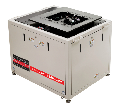
InfraScan(TM) ES400C-LW Emission Solution for Lower Voltage IC Designs (Photo: Business Wire)
InfraScan™ ES400C-LW was developed to meet the demands of the newest lower power IC designs and architectures. These smaller geometries and lower voltages ICs require emission tools that are capable of seeing emissions that are further into the infrared regime than the traditional InGaAs cameras can detect. Checkpoint’s newly designed MCT camera and optical system offers proprietary improvements for use with its solid immersion lens objective. This state-of-the-art design allows users 30-minute exposures of their devices. Checkpoint’s MCT camera is capable of viewing emissions from 900 nm to 2500 nm, allowing users to see photon emission and thermal imaging from the same tool. The new InfraScan ES400C-LW camera is equipped with an optical filter wheel that allows the user to select the appropriate emission regime for the design that is under test. In 2013, Checkpoint introduced the first production 3.3 NA SIL objective offering the highest NA available. Checkpoint’s 3.3 NA SIL has been used successfully in the field for debugging 14 nm designs for over a year now. Checkpoint has also enhanced the illumination portion of the InfraScan ES400C-LW offering a 25% increase in optical resolution.
“The InfraScan ES400C-LW is the logical next step for emission tools to meet the demands of lower voltage IC architectures,” said Michael Jupina, Checkpoint Technologies General Manager. “By increasing the wavelength regime, resolution and integration time, simultaneously.” Dr. Jupina went on to say that, “Checkpoint has, once again, reiterated its place as the market leader in the IC debugging and imaging field.”
The improvements designed for the new stand-alone emission platform are also available in the full laser and emission combination platform. Checkpoint’s InfraScan™ ES400C-LW is capable of being equipped with the MCT camera, 3.3 NA SIL and a complete laser scanning microscope with passive, active and laser probing of devices. This single system is capable of performing all optical debugging and failure analysis techniques.
About Checkpoint Technologies
Founded in 1995, Checkpoint Technologies develops and manufactures optical failure analysis tools used by semiconductor manufacturers to improve the speed and reliability of integrated circuits for the failure analysis industry. Headquartered in San Jose, California USA with worldwide sales and service. www.checkpointtechnologies.com
Photos/Multimedia Gallery Available: http://www.businesswire.com/multimedia/home/20141111005374/en/
Contact:
Checkpoint Technologies, LLC
Michael Jupina, 408-321-9780 ext. 102
Email Contact