STMicroelectronics expands into 3D depth sensing
with latest time-of-flight sensors
- Building on a leading position in direct Time-of-Flight sensors, with two billion FlightSense™ devices sold, ST reveals new direct and indirect Time-of-Flight sensors for key applications like camera assist, virtual reality, 3D webcam, robotics and smart buildings
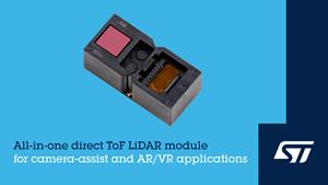
- Market-first true all-in-one dToF LiDAR module with up to 2.3k zones, targets smartphone camera-assist and AR/VR applications
- The world’s smallest iToF sensor with 672x804-pixel resolution, is now in volume production with a first design win at Lanxin Technology
Geneva, Switzerland, February 22, 2024 – STMicroelectronics (NYSE: STM), a global semiconductor leader serving customers across the spectrum of electronics applications, announced an all-in-one, direct Time-of-Flight (dToF) 3D LiDAR (Light Detection And Ranging) module with market-leading 2.3k resolution, and revealed an early design win for the world's smallest 500k-pixel indirect Time-of-Flight (iToF) sensor.
“ToF sensors, which can accurately measure the distance to objects in a scene, are driving exciting new capabilities in smart devices, home appliances, and industrial automation. We have already delivered two billion sensors into the market and continue to extend our unique portfolio, which covers all types from the simplest single-zone devices up to our latest high-resolution 3D indirect and direct ToF sensors,” said Alexandre Balmefrezol, General Manager, Imaging Sub-Group at STMicroelectronics. “Our vertically integrated supply chain, covering everything from pixel and metasurface lens technology and design to fabrication, with geographically diversified in-house high-volume module assembly plants, lets us deliver extremely innovative, highly integrated, and high-performing sensors.”
The VL53L9, announced today, is a new direct ToF 3D LiDAR device with a resolution of up to 2.3k zones. Integrating a dual scan flood illumination, unique in the market, the LiDAR can detect small objects and edges and captures both 2D infrared (IR) images and 3D depth map information. It comes as a ready-to-use low power module with its on-chip dToF processing, requiring no extra external components or calibration. Additionally, the device delivers state-of-the-art ranging performance from 5cm to 10 meters.
VL53L9’s suite of features elevates camera-assist performance, supporting macro up to telephoto photography. It enables features such as laser autofocus, bokeh, and cinematic effects for still and video at 60fps (frame per second). Virtual reality (VR) systems can leverage accurate depth and 2D images to enhance spatial mapping for more immersive gaming and other VR experiences like virtual visits or 3D avatars. In addition, the sensor’s ability to detect the edges of small objects at short and ultra-long ranges makes it suitable for applications such as virtual reality or SLAM (simultaneous localization and mapping).
ST is also announcing news of its VD55H1 ToF sensor, including the start of volume production and an early design win with Lanxin Technology, a China-based company focusing on mobile-robot deep-vision systems. MRDVS, a subsidiary company, has chosen the VD55H1 to add high-accuracy depth-sensing to its 3D cameras. The high-performance, ultra-compact cameras with ST’s sensor inside combine the power of 3D vision and edge AI, delivering intelligent obstacle avoidance and high-precision docking in mobile robots.
In addition to machine vision, the VD55H1 is ideal for 3D webcams and PC applications, 3D reconstruction for VR headsets, people counting and activity detection in smart homes and buildings. It packs 672 x 804 sensing pixels in a tiny chip size and can accurately map a three-dimensional surface by measuring distance to over half a million points. ST’s stacked-wafer manufacturing process with backside illumination enables unparalleled resolution with smaller die size and lower power consumption than alternative iToF sensors in the market. These characteristics give the sensors their excellent credentials in 3D content creation for webcams and VR applications including virtual avatars, hand modeling and gaming.
First samples of the VL53L9 are already available for lead customers and mass production is scheduled for early 2025. The VD55H1 is in full production now.
Pricing information and sample requests are available at local ST sales offices.
ST will showcase a range of ToF sensors including the VL53L9 and explain more about its technologies at Mobile World Congress 2024, in Barcelona, February 26-29, at booth 7A61.
Notes to Editors
Time-of-flight (ToF) sensors use photon travel time between two points to calculate the distance between those points.
3D ToF depth sensors provide a map of ranging information computing the distance to multiple objects in the field-of-view. With flood illumination, 3D sensors are also able to acquire an IR 2D frame used to improve the post-processing and so enrich the user experience. 3D ToF sensors can map a scene for robot navigation and collision avoidance, detect and localize objects or people for smart building applications such as room-usage analysis and emergency assistance. Combining a 3D ToF rendering with the output of a color image sensor gives the opportunity to create truly immersive virtual reality experiences.
The VD55H1 calculates the distance to points on a surface by measuring the phase shift between its emitted signal and the received, reflected signal. This indirect Time-of-Flight (iToF) sensing is a complementary technique to direct Time-of-Flight (dToF) sensing used by sensors like the VL53L9, which measures the time between transmitting and receiving the reflected signals. ST’s broad portfolio of advanced technologies enables the Company to design both direct and indirect high-resolution ToF sensors, and offer optimized solutions tailored to application requirements.
About STMicroelectronics
At ST, we are over 50,000 creators and makers of semiconductor technologies mastering the semiconductor supply chain with state-of-the-art manufacturing facilities. An integrated device manufacturer, we work with more than 200,000 customers and thousands of partners to design and build products, solutions, and ecosystems that address their challenges and opportunities, and the need to support a more sustainable world. Our technologies enable smarter mobility, more efficient power and energy management, and the wide-scale deployment of cloud-connected autonomous things. We are committed to achieving our goal to become carbon neutral on scope 1 and 2 and partially scope 3 by 2027. Further information can be found at
www.st.com.
For Press Information Contact:
Alexis Breton
Corporate External Communications
Tel: +33.6.59.16.79.08
alexis.breton@st.com
Attachments
- P4608D -- Feb 22 2024 -- VD55H1 and VL53L9 ToF sensors_FINAL FOR PUBLICATION
- P4608D -- Feb 22 2024 -- VD55H1 and VL53L9 ToF sensors_IMAGE


