Highlights
- Archer Materials’ commercial foundry partner in the Netherlands has validated its advanced biochip gFET design by manufacturing the chips using whole four-inch wafer semiconductor fabrication processes.
- The new gFET design for multiplexing was fabricated at a commercial scale foundry.
- The validation of the new advanced gFET device design and whole wafer run in a commercial foundry represents a critical milestone in the commercialisation pathway for Archer’s biochip.
- Archer now intends to integrate more functionality on the biochip, and optimise the device size and geometry to build advanced sensing regions.
- The biochip designs and devices form the basis of intellectual property that is 100% owned by Archer.
SYDNEY, Australia, Sept. 13, 2023 (GLOBE NEWSWIRE) -- Archer Materials Limited (“Archer”, the “Company”, “ ASX: AXE”), a semiconductor company advancing the quantum computing and medical diagnostics industries, has had its advanced graphene field effect transistor (“gFET”) chip design validated by a commercial foundry partner in the Netherlands with a whole four-inch wafer run.
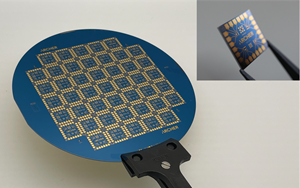
The new advanced gFET device designs have been fabricated and the whole wafer run foundry process was successful (Image 1). The electronic and spectroscopic characteristics of the gFET chips, and the foundry fabrication process yield, are consistent with what Archer expected. The gFET chips are also compatible with Archer’s biochip system platform.
The advanced gFET design now creates the potential for an early biochip platform that has single-device multiplexing, meaning the biochip technology would be able to sense different liquid samples to test for multiple diseases at once. Archer now intends to integrate more functionality on the biochip, and optimise the device size and geometry to build advanced sensing regions.
Commenting on the validation of the advanced gFET design, Dr Mohammad Choucair, CEO of Archer, said, “Archer’s biochip graphene sensor technology has essentially undergone translation from design to scalable semiconductor processing in a commercial foundry, which is both a key technology development and commercial milestone.
“The whole wafer fabrication of the gFET device design is a significant step towards industrial production. Archer is continuing to strengthen its relationships with global foundry partners to deliver these chips using a streamlined ‘fabless’ commercialisation model.”
Image 1. Archer’s advanced gFET chip for advanced biosensing diced from the whole four-inch wafer fabricated in a commercial foundry.
Background
On 31 July 2023, Archer announced that its advanced gFET design had been sent to a commercial foundry partner in the Netherlands for a whole four-inch wafer run for validation. In parallel, Archer’s first-generation gFET design was submitted to a commercial foundry partner in Germany for a Multi-Project Wafer (“MPW”) run which is expected to be completed by the end of 2023, as announced on 13 July 2023. An MPW is where Archer’s device design is imprinted on a small area of a wafer with the designs of other companies on the same wafer. The MPW fabrication is independent to Archer’s dedicated whole wafer run.
| The Board of Archer authorised this announcement to be given to ASX. | |
|
Investor enquiries
Eric Kuret +61 417 311 335 Email Contact |
Media enquiries
Tristan Everett +61 403 789 096 Email Contact |
About Archer
Archer is a technology company that operates within the semiconductor industry. The Company is developing advanced semiconductor devices, including chips relevant to quantum computing and medical diagnostics. Archer utilises its global partnerships to develop these technologies for potential deployment and use across multiple industries. www.archerx.com.au
A photo accompanying this announcement is available at https://www.globenewswire.com/NewsRoom/AttachmentNg/ddb3777a-7d26-4648-a324-69439df923e3


