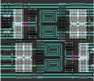
Samsung designers will leverage Ansys' EM design tools, Ansys RaptorX, Ansys VeloceRF, and Ansys Exalto, to help reduce time to market by two to three weeks on smaller designs and up to two months for complex designs. With automation capabilities that optimize calculations and modeling, coupled with larger capacity, Ansys' software will allow the Samsung team to design at faster speeds with higher fidelity.
"Electronic systems and process technologies are constantly evolving and therefore require leading-edge EM design capabilities," said Sangyun Kim, corporate vice president of the Foundry Design Technology Team at Samsung Electronics. "We believe that Ansys' simulation solutions meet these challenges and will deliver the highest level of proficiency for our design needs, while reducing design time, cost, and risk."
By integrating Ansys' EM solutions, Samsung designers can model complex on-chip scenarios, including dummy tiles, which comprise millions of metal pieces in a fraction of the time. Additionally, Ansys' near real-time modelling capabilities safeguard designs from EM interference, which helps significantly lower the risk of chip failure.
"EM is a primary challenge for chip designers as connectivity demands increase and technologies advance worldwide," said John Lee, vice president and general manager of the electronics, semiconductor, and optics business unit at Ansys. "At Ansys, we ensure that our simulation solutions not only meet these rising demands but remain ahead of them. We are confident that Ansys' EM design portfolio is well-equipped to serve the Samsung team with the tools they need to optimize their on-chip designs."
Ansys and Samsung have a long history of collaboration that delivers advanced solutions, including power integrity and electromigration signoff solutions for low-power mobile and high-performance computing applications.
When visionary companies need to know how their world-changing ideas will perform, they close the gap between design and reality with Ansys simulation. For more than 50 years, Ansys software has enabled innovators across industries to push boundaries by using the predictive power of simulation. From sustainable transportation to advanced semiconductors, from satellite systems to life-saving medical devices, the next great leaps in human advancement will be powered by Ansys.
Take a leap of certainty … with Ansys.
Ansys and any and all ANSYS, Inc. brand, product, service and feature names, logos and slogans are registered trademarks or trademarks of ANSYS, Inc. or its subsidiaries in the United States or other countries. All other brand, product, service and feature names or trademarks are the property of their respective owners.
ANSS–T
Contacts |
|
Media | Mary Kate Joyce |
|
| 724.820.4368 |
|
| |
|
|
|
Investors | Kelsey DeBriyn |
|
| 724.820.3927 |
|
|
![]() View original content to download multimedia:
https://www.prnewswire.com/news-releases/samsung-adopts-ansys-simulation-portfolio-to-create-semiconductor-designs-to-optimize-high-speed-connectivity-301581735.html
View original content to download multimedia:
https://www.prnewswire.com/news-releases/samsung-adopts-ansys-simulation-portfolio-to-create-semiconductor-designs-to-optimize-high-speed-connectivity-301581735.html
SOURCE Ansys
| Contact: |
| Company Name: Ansys
Financial data for Ansys |


