SANTA CLARA, Calif., March 22, 2022 (GLOBE NEWSWIRE) --
GTC—Enabling a new generation of system-level integration in data centers, NVIDIA today announced
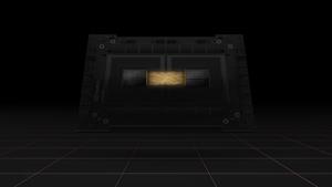
NVIDIA® NVLink®-C2C, an ultra-fast chip-to-chip and die-to-die interconnect that will allow custom dies to coherently interconnect to the company’s GPUs, CPUs, DPUs, NICs and SOCs.
With advanced packaging, NVIDIA NVLink-C2C interconnect would deliver up to 25x more energy efficiency and be 90x more area-efficient than PCIe Gen 5 on NVIDIA chips and enable coherent interconnect bandwidth of 900 gigabytes per second or higher.
“Chiplets and heterogeneous computing are necessary to counter the slowing of Moore’s law,” said Ian Buck, vice president of Hyperscale Computing at NVIDIA. “We’ve used our world-class expertise in high-speed interconnects to build uniform, open technology that will help our GPUs, DPUs, NICs, CPUs and SoCs create a new class of integrated products built via chiplets.”
NVIDIA NVLink-C2C is the same technology that is used to connect the processor silicon in the NVIDIA Grace™ Superchip family, also announced today, as well as the Grace Hopper Superchip announced last year. NVLink-C2C is now open for semi-custom silicon-level integration with NVIDIA technology.
NVIDIA NVLink-C2C supports the Arm® AMBA® Coherent Hub Interface (AMBA CHI) protocol. NVIDIA and Arm are working closely together to enhance AMBA CHI to support fully coherent and secure accelerators with other interconnected processors.
“As the future of CPU design is increasingly accelerated and multichip, it is critical to support chiplet-based SoCs across the ecosystem,” said Chris Bergey, senior vice president and general manager of the Infrastructure Line of Business at Arm. “Arm is supporting a broad set of connectivity standards and designing our AMBA CHI protocol to support these future technologies, including collaborating with NVIDIA on NVLink-C2C to address use cases like coherent connectivity between CPUs, GPUs and DPUs.”
NVIDIA NVLink-C2C is built on top of NVIDIA’s world-class SERDES and LINK design technology, and it is extensible from PCB-level integrations and multichip modules to silicon interposer and wafer-level connections, delivering extremely high bandwidth while optimizing for energy and die area efficiency.
In addition to NVLink-C2C, NVIDIA will also support the developing Universal Chiplet Interconnect Express (UCIe) standard announced earlier this month. Custom silicon integration with NVIDIA chips can either use the UCIe standard or NVLink-C2C, which is optimized for lower latency, higher bandwidth and greater power efficiency.
Some of NVLink-C2C’s key features include:
- High Bandwidth – supporting high-bandwidth coherent data transfers between processors and accelerators
- Low Latency – supporting atomics between processors and accelerators to perform fast synchronization and high-frequency updates to shared data
- Low Power and High Density – using advanced packaging, it is 25x more energy efficient and 90x more area-efficient than PCIe Gen 5 on NVIDIA chips
- Industry-Standard Support – works with Arm’s AMBA CHI or CXL industry-standard protocols for interoperability between devices
To learn more about NVIDIA NVLink C2C, watch NVIDIA CEO Jensen Huang’s keynote address at GTC 2022. Register for GTC for free to attend sessions with NVIDIA and industry leaders.
About NVIDIA
NVIDIA’s (NASDAQ: NVDA) invention of the GPU in 1999 sparked the growth of the PC gaming market and has redefined modern computer graphics, high performance computing, and artificial intelligence. The company’s pioneering work in accelerated computing and AI is reshaping trillion-dollar industries, such as transportation, healthcare and manufacturing, and fueling the growth of many others. More information at
https://nvidianews.nvidia.com/.
For further information, contact:
Cliff Edwards
Enterprise PR
NVIDIA Corporation
+1-415-699-2755
Email Contact
Certain statements in this press release including, but not limited to, statements as to: the benefits, impact, specifications, performance and availability of NVIDIA NVLink-C2C; chiplets and heterogeneous computing being necessary to counter the slowing of Moore’s law; our building of uniform, open technology helping our GPUs, DPUs, NICs, CPUs and SoCs create a new class of integrated products built via chiplets; NVIDIA’s collaboration with Arm leading to future Arm AMBA CHI enhancements; NVIDIA’s support of the UCIe standard and its impact; and custom silicon integrators being able to use NVIDIA CPUs, GPUs, DPUs, NIC and SOCs for either NVLink-C2C or UCIe are forward-looking statements that are subject to risks and uncertainties that could cause results to be materially different than expectations. Important factors that could cause actual results to differ materially include: global economic conditions; our reliance on third parties to manufacture, assemble, package and test our products; the impact of technological development and competition; development of new products and technologies or enhancements to our existing product and technologies; market acceptance of our products or our partners' products; design, manufacturing or software defects; changes in consumer preferences or demands; changes in industry standards and interfaces; unexpected loss of performance of our products or technologies when integrated into systems; as well as other factors detailed from time to time in the most recent reports NVIDIA files with the Securities and Exchange Commission, or SEC, including, but not limited to, its annual report on Form 10-K and quarterly reports on Form 10-Q. Copies of reports filed with the SEC are posted on the company's website and are available from NVIDIA without charge. These forward-looking statements are not guarantees of future performance and speak only as of the date hereof, and, except as required by law, NVIDIA disclaims any obligation to update these forward-looking statements to reflect future events or circumstances.
© 2022 NVIDIA Corporation. All rights reserved. NVIDIA, the NVIDIA logo, NVIDIA Grace and NVLink are trademarks and/or registered trademarks of NVIDIA Corporation in the U.S. and other countries. All other trademarks and copyrights are the property of their respective owners. Features, pricing, availability, and specifications are subject to change without notice.
A photo accompanying this announcement is available at https://www.globenewswire.com/NewsRoom/AttachmentNg/4503f21b-03db-45f6-aa86-e3887f3d8f88


