TAMPERE, Finland — (BUSINESS WIRE) — December 13, 2021 — The first System on Chip (SoC) developed by the Finnish SoC Hub consortium has been taped out. The project partners will focus next on improving the design, automation and performance of the SoC. The first of the three chips to be developed by the consortium will be ready for deployment in early 2022. The project contributes to strengthening Europe’s technological sovereignty.
This press release features multimedia. View the full release here: https://www.businesswire.com/news/home/20211213005527/en/

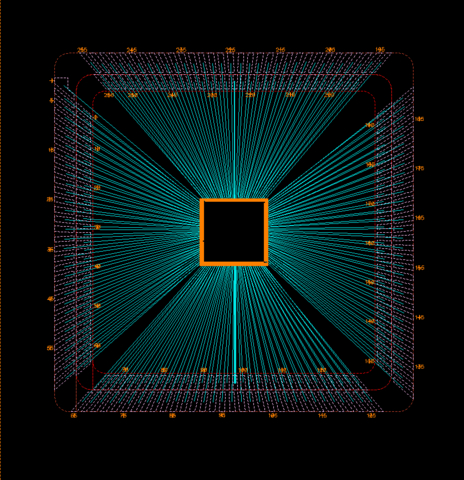
The bonding diagram image shows how the chip IO pads are wired to the package pins. The package is soldered to the printed circuit board. The layout picture depicts how the functional blocks are physically located on the chip. The IO pads that are bonded to the package pins are shown on the sides. Photos: SoC Hub. (Graphic: Business Wire)
The Finnish SoC Hub has set out to develop the domain of SoC design as a pioneer in Europe and to enhance Finland’s competitive position. The SoC Hub initiative, coordinated by Tampere University, Finland, and Nokia, was launched last year. The co-creation activities carried out by the partners go well beyond the scope of a conventional research project.
“The SoC has been developed using the same methods that are used in industrial production, such as design for testability, extensive verification and focusing on system-level integration instead of single modules,” says Ari Kulmala, professor of practice in SoC design at Tampere University.
According to Kulmala, the chip can also be tested by external stakeholders as it includes a development kit, and it can be integrated into a wide range of other systems.
One of the key goals of the SoC Hub project is to enable rapid prototyping for new ideas, for example, in the Internet of things (IoT), machine learning and 5G and 6G technologies in silicon.
The newly taped-out Ballast chip is the first in a series of three chips. The chip will be manufactured by TSMC, the world’s largest manufacturer of semiconductor chips.
The chip is manufactured using TSMC’s recent 22nm Ultra Low Leakage process, which is especially well suited for IoT and Edge devices. Ballast contains several different RISC-V CPU cores, a Digital Signal Processor, an AI accelerator, rich sensor-like interfaces and an extension interface to FPGA. A full software stack – including drivers, software development tools and chip debugging support – has also been implemented. The chip supports both real-time operating systems and Linux simultaneously.
“It has been a pleasure to work with the SoC Hub team. They have been extremely quick to develop the chip, and the quality of the work has been top class,” says Bas Dorren, Director of Business Development at imec.IC-link, part of imec (an R&D hub for nano and digital technologies).
Another two chips taped out in the next two years
Considering its large size, the chip was created in a very short time. The ambitious goal was achieved thanks to the good team spirit and the expertise and experience of the specialists involved.
“A great deal of work has been done to enable seamless collaboration between the University and company partners. Several early career researchers have participated in designing Ballast and have therefore had the opportunity to apply the knowledge they acquired from their studies in an industrial project,” says Timo Hämäläinen, head of the Computing Sciences Unit at Tampere University.
Besides the development of the SoC, the first phase of the project was also a major undertaking, involving building the consortium and the preparation of the necessary software and licence agreements. Headed by Tampere University and Nokia, the consortium comprises CoreHW, VLSI Solution, Siru Innovations, TTTEch Flexibilis, Procemex, Wapice and Cargotec as partners.
In the project funded by Business Finland, three SoCs will be taped out by the end of 2023. Use cases for the chips will be planned together with the project consortium.
“In the next phases of the project, we will be able to focus even more on the systematics, automation and performance of the SoCs. Despite having achieved our first goal, we continue moving forward right away. The time to invest in SoC development is now, not tomorrow,” emphasises Timo Hämäläinen.
Tampere University
The multidisciplinary Tampere University is the second largest university in Finland. The spearheads of our research and learning are technology, health and society. The University is committed to addressing the greatest challenges that are facing our society and creating new opportunities. Almost all the internationally recognised fields of study are represented at the University. Together, Tampere University and Tampere University of Applied Sciences comprise the Tampere Universities community made up of more than 30,000 students and close to 5,000 employees. www.tuni.fi/en
View source version on businesswire.com: https://www.businesswire.com/news/home/20211213005527/en/
Contact:
Inquiries:
SoC Hub consortium
sochub@tuni.fi
Timo Hämäläinen
Head of the Computing Sciences Unit at Tampere University
timo.hamalainen@tuni.fi
Ari Kulmala
Professor of practice in System-on-Chip design at Tampere University
ari.kulmala@tuni.fi


