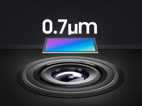
Compact chips boast industry’s smallest pixel size, allowing sleeker designs and minimized camera bumps
The new 0.7μm lineup will adopt enhanced pixel technology with boosted light sensitivity, ISOCELL 2.0, later this year
SEOUL, South Korea — (BUSINESS WIRE) — September 15, 2020 — Samsung Electronics Co., Ltd., a world leader in advanced semiconductor technology, today introduced four new Samsung ISOCELL image sensors for its 0.7 micrometer (μm)-pixel product lineup; 108-megapixel (Mp) ISOCELL HM2, 64Mp ISOCELL GW3, 48Mp ISOCELL GM5 and 32Mp ISOCELL JD1. With the new 0.7μm ISOCELL technology, Samsung plans to expand the ultra-high-resolution offerings to mainstream smartphones.
This press release features multimedia. View the full release here: https://www.businesswire.com/news/home/20200915005521/en/

Samsung ISOCELL 2.0 (Photo: Business Wire)
“Samsung continues to pioneer innovations, such as ISOCELL Plus and Smart ISO, to deliver more pixels in a smaller package,” said Yongin Park, executive vice president of the sensor business at Samsung Electronics. “Last year, Samsung introduced the industry’s first 0.7μm-pixel image sensor and the first 108Mp sensors. Now we are bringing more of the advanced pixel technologies to mobile cameras in a variety of options that will enable high-resolution images and sleeker designs in a wider selection of tomorrow’s mobile devices.”
For ultra-high-resolution image sensors, even a mere 0.1μm-difference per pixel can have a significant impact on the overall size of the sensor as well as the height of the camera module. With pixels at 0.7μm, Samsung’s newest image sensors are up to 15-percent smaller than the 0.8μm sensors of the same resolution and reduce the height of the camera module by up to 10 percent. Smaller form factors give smartphone manufacturers more flexibility, such as added features or more streamlined designs, when developing their next-generation devices.
To collect an ample amount of light and increase the full well capacity despite the minute pixel sizes, Samsung has incorporated its advanced ISOCELL Plus and Smart-ISO technologies, especially optimized for 0.7μm. ISOCELL Plus retains the received light with a wall-like structure around the pixel while Smart-ISO makes full use of the incoming light by intelligently adjusting the ISO accordingly for optimal exposure.
In the latest 0.7μm products to be introduced later this year, Samsung will start rolling out an enhanced pixel technology, ISOCELL 2.0, which allows excellent performance despite the challenges with decreasing pixel sizes. The new technology further enhanced the wall structure between cells, resulting in added light sensitivity of up to 12 percent compared to the current ISOCELL Plus technology.
The New 0.7μm Lineup;
- ISOCELL HM2 is Samsung’s third 108Mp image sensor following the HMX and HM1. The new 108Mp-sensor is around 15-percent smaller than the 0.8μm-based predecessors, and reduces the height of the camera module by 10 percent. The HM2 features Super PD, a faster and more effective phase detecting auto focus solution, and like the HM1, comes with a nine-pixel binning technology as well as 3x lossless zoom.
- ISOCELL GW3 is a 64Mp-image sensor optimized for mainstream devices. Thanks to the smaller pixel size, the GW3’s optical size is nearly identical to that of Samsung’s 0.8μm 48Mp image sensor. In addition to Tetracell and Smart-ISO technologies that help the sensor take bright images with high color fidelity, the GW3 is ideal for active lifestyles, featuring gyro-based electronic image stabilization (EIS) for sharper still photos and steadier videos. The image sensor supports video recording at up to 4K resolution at 60 frames-per-second (fps).
- ISOCELL GM5 is a versatile 48Mp-image sensor designed for use in telescoping or ultra-wide angle cameras. When used as a 5x optical telescoping sensor for folded-zoom, the GM5 takes full advantage of the compact 0.7μm pixel size that minimizes the camera bulge. For ultra-wide shots, the GM5 supports high-speed full-HD recording at 480fps. The sensor also offers a staggered-HDR feature, a faster and more power-efficient HDR technology that expedites image processing by sending a readout of long, medium, and short exposures of each row of pixels respectively to the mobile processor. As the readout is performed based on Tetracell’s 1.4μm two-by-two pixels, rather than at the individual 0.7μm-pixel level, staggered-HDR can provide brighter and clearer images with less noise.
- ISOCELL JD1 is the industry’s smallest 32Mp-image sensor at 1/3.14-inches, making it an ideal solution for smartphones with bezel-less displays that incorporate a hole-in-active-area or motorized pop-up mechanism for the front-facing camera. Even with 32-million pixels to capture a highly detailed selfie, the camera sits comfortably under the display as the height of the sensor’s camera module is comparable to those of 0.9μm 20Mp or 1.0μm 16Mp sensors. Like the GM5, the JD1 is also the one the first ISOCELL image sensors to offer staggered-HDR.
Samsung ISOCELL HM2, GW3 and JD1 are currently in mass production, and the company is sampling GM5.
# # #
About Samsung Electronics Co., Ltd.
Samsung inspires the world and shapes the future with transformative ideas and technologies. The company is redefining the worlds of TVs, smartphones, wearable devices, tablets, digital appliances, network systems, and memory, system LSI, foundry and LED solutions. For the latest news, please visit the Samsung Newsroom at http://news.samsung.com.
# # #
* Samsung first announced its ISOCELL technology in 2013, which reduces color crosstalk between pixels by placing a physical barrier, allowing small-sized pixels to achieve higher color fidelity. Based on this technology, Samsung introduced the industry’s first 1.0um-pixel image sensor in 2015 and a 0.9-pixel sensor in 2017. In June 2018, Samsung introduced an upgraded pixel isolation technology, the ISOCELL Plus.
View source version on businesswire.com: https://www.businesswire.com/news/home/20200915005521/en/
Contact:
Ujeong Jahnke
Samsung Semiconductor Europe GmbH
Tel. +49(0)89-45578-2092
Email:
ujeong.j@samsung.com


