Challenges and Solutions Revealed for the First Time at TSMC's OIP Ecosystem Forum
MILPITAS, Calif., Aug. 25, 2020 — (PRNewswire) — Alchip Technologies today revealed the trials, tribulation and victories inherent in the production of huge reticle-size processors that power today's most advanced supercomputers.In a technical paper delivered at TSMC's virtual OIP Ecosystem Forum entitled Reticle Size Design and Chiplet Capabilities, James Huang Alchip's Vice President of R&D, discusses designing an 85x85mm machine learning processor that registered a world-record 21.11 GFLOPS/Watt power efficiency.
The record-setting device consisted of four identical 1.6B gate die manufactured on TSMC's 12nm process technology, each supporting 180MB of SRAM and 204 GBs of memory bandwidth. The dice are connected by die-to-die APLink 1.0 PHY IP.
"Machine learning chips tend to have distributed memories and each machine learning core has its localized memories and MAC with input data streamed into each core through an NoC. Machine learning chip performance is highly dependent on each core's speed and power efficiency," Mr. Huang explained.
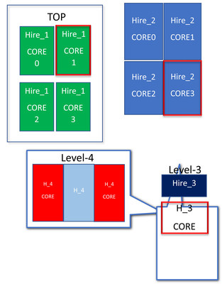
Physical design challenges included multi-level logic and physical hierarchy with thousands of repeated cores that called for a symmetrical channel-less floorplan and a redundancy strategy for yield optimization and data bus traffic. Other challenges included extremely high static and dynamic power consumption, clock network design, power distribution, network design, PCB/Package/SoC co-design and thermal considerations.
Alchip met the challenge with a clock design strategy that called for a fishbone clock scheme that included chip-level clock phase control with the clock network divided into various phase shift groups and peak current analysis and control. The strategy also called for custom decoupling cells and MIM caps for critical clock and power.
The design also called for a custom DFT redundancy strategy for critical and non-critical logic so that multiple defective cores could be detected and repaired. An adaptive high-bandwidth test also leveraged functional high-speed interfaces for structural tests and extremely high-bandwidth that reduces test time.
At the backend, designers integrated four homogeneous chiplets on an 8-2-8 organic substrate that utilized a proprietary die-to-die I/0 interface with a bandwidth of 576Gbps per die-to-die channel.
"Because this is a complex, full reticle sized SoC, it created a number of design challenges. Chief among them is providing heat dissipation for the enormous 500-watt power consumption" explained Johnny Shen, CEO, Alchip Technologies. "We developed mechanical package samples at the very early stage to eliminate the reliability concerns of mounting such a large chip. This complicated test design was a particularly challenging, given the project's tight schedule," he explained.
For more information, go to www.alchip.com.
About Alchip
Alchip Technologies Ltd., headquartered in Taipei, Taiwan, is a leading global provider of silicon design and production services for system companies developing complex and high-volume ASICs and SoCs. The company was founded by semiconductor veterans from Silicon Valley and Japan in 2003 and provides faster time-to-market and cost-effective solutions for SoC design at mainstream and advanced, including 7nm processes. Customers include global leaders in AI, HPC/supercomputer, mobile phones, entertainment device, networking equipment and other electronic product categories. Alchip is listed on the Taiwan Stock Exchange (TWSE: 3661) and is a TSMC-certified Value Chain Aggregator.
![]() View original content to download multimedia:
http://www.prnewswire.com/news-releases/alchip-technologies-reveals-secrets-behind-reticle-size-design-301118009.html
View original content to download multimedia:
http://www.prnewswire.com/news-releases/alchip-technologies-reveals-secrets-behind-reticle-size-design-301118009.html
SOURCE Alchip Technologies Ltd
| Contact: |
| Company Name: Alchip Technologies Ltd
Chuck Byers Email Contact +1-408-310-9244 Web: http://www.alchip.com Financial data for Alchip Technologies Ltd |


