

"Sensor solutions require performance and reliability levels far above those of commercial components," said HENSOLDT CEO, Thomas Müller. "To have high-density components quickly available with reduced effort by means of 3D printing gives us a competitive edge in the development process of such high-end electronic systems."
"Nano Dimension's relationship with HENSOLDT is the type of partnership with customers we are striving for," commented Yoav Stern, Nano Dimension President & CEO. "Working together and learning from HENSOLDT led us to reach a first-of-its-kind in-depth knowledge of polymer materials applications. Additionally, it guided us in the development of Hi-PEDs (High Performance Electronic Device) that create competitive edges by enabling unique implementations with shortest time to market."
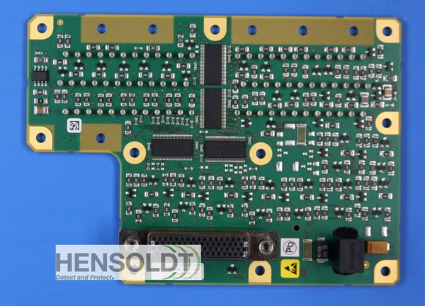
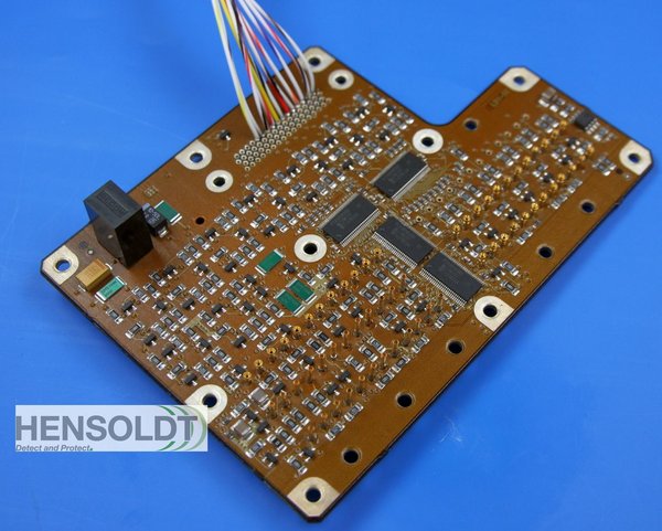
AMEs are useful to verify a new design and functionality of specialized electronic components before production. AME is a highly agile and individual engineering methodology to prototype a new electronic circuitry. This leads to significant reduction of time and cost in the development process. Furthermore, AME gives a verified and approved design before production starts, leading to higher quality of the final product.
HENSOLDT started working with Nano Dimension's DragonFly 3D printing system in 2016, in order to examine the possibilities of 3D printing electronics. Last year, HENSOLDT successfully implemented the DragonFly Lights-Out Digital Manufacturing (LDM) printing technology, the industry's only additive manufacturing platform for round-the-clock 3D printing of electronic circuitry.
About HENSOLDT
HENSOLDT is a pioneer of technology and innovation in the field of defence and security electronics. Based in Taufkirchen near Munich, the company is a German Champion with strategic leadership positions in the field of sensor solutions for defence and non-defence applications. HENSOLDT develops new products to combat a wide range of threats based on innovative approaches to data management, robotics and cyber security. With approximately 5,500 employees, HENSOLDT generated revenues of 1.14 billion euros in 2019. www.hensoldt.net
About Nano Dimension
Nano Dimension (Nasdaq, TASE: NNDM) is a provider of intelligent machines for the fabrication of Additively Manufactured Electronics (AME). High fidelity active electronic and electromechanical subassemblies are integral enablers of autonomous intelligent drones, cars, satellites, smartphones, and in vivo medical devices. They necessitate iterative development, IP safety, fast time-to-market and device performance gains, thereby mandating AME for in-house, rapid prototyping and production. Nano Dimension machines serve cross-industry needs by depositing proprietary consumable conductive and dielectric materials simultaneously, while concurrently integrating in-situ capacitors, antennas, coils, transformers and electromechanical components, to function at unprecedented performance. Nano Dimension bridges the gap between PCB and semiconductor integrated circuits. A revolution at the click of a button: From CAD to a functional high-performance AME device in hours, solely at the cost of the consumable materials.
For more information, please visit www.nano-di.com.
Forward-Looking Statements
This press release contains forward-looking statements within the meaning of the "safe harbor" provisions of the Private Securities Litigation Reform Act of 1995 and other Federal securities laws. Words such as "expects," "anticipates," "intends," "plans," "believes," "seeks," "estimates" and similar expressions or variations of such words are intended to identify forward-looking statements. For example, Nano Dimension is using forward-looking statements in this press release when it discusses the benefits and potential of its products. Because such statements deal with future events and are based on Nano Dimension's current expectations, they are subject to various risks and uncertainties. Actual results, performance or achievements of Nano Dimension could differ materially from those described in or implied by the statements in this press release. The forward-looking statements contained or implied in this press release are subject to other risks and uncertainties, including those discussed under the heading "Risk Factors" in Nano Dimension's annual report on Form 20-F filed with the Securities and Exchange Commission ("SEC") on March 14, 2019, and in any subsequent filings with the SEC. Except as otherwise required by law, Nano Dimension undertakes no obligation to publicly release any revisions to these forward-looking statements to reflect events or circumstances after the date hereof or to reflect the occurrence of unanticipated events. References and links to websites have been provided as a convenience, and the information contained on such websites is not incorporated by reference into this press release. Nano Dimension is not responsible for the contents of third-party websites.
Photo -
https://photos.prnasia.com/prnh/20200520/2809231-1-a
Photo -
https://photos.prnasia.com/prnh/20200520/2809231-1-b
Logo -
https://photos.prnasia.com/prnh/20190905/2570842-1LOGO
SOURCE Nano Dimension
| Contact: |
| Company Name: Nano Dimension, HENSOLDT
HENSOLDT, Lothar Belz Phone: +49 (0)731.392.3681 Email Contact NANO DIMENSION, ASIA-PACIFIC CONTACT, Tracy Tsang , APAC Marketing & Business Operation Manager, tracy@nano-di.com; INVESTOR RELATIONS CONTACT, Yael Sandler, CFO, ir@nano-di.com Web: http://www.nano-di.com Financial data for Nano Dimension, HENSOLDT |


