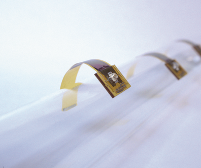
Innovative packaging enabled by Nano Dimension's AME technology
BOCA RATON, Fla., April 16, 2020 — (PRNewswire) — Nano Dimension Ltd. (Nasdaq, TASE: NNDM), a leading Printed electronics (PE) / Additively Manufactured Electronics (AME) provider, announced today that its technology, DragonFly LDM system and materials were used to develop a 3D printed sealed packaging with electrical pads for Micro-Electromechanical Systems (MEMS).

The printed electronics package has the electrical pads directly printed on the metal layers on which an RF connector is soldered. The ability to transfer electric pads in a sealed package is one of the most crucial parts in ohmic-contact microelectromechanical systems (MEMS) as it determines the device performance and reliability, particularly for soft and flexible devices where the electrical connectors are typically difficult to produce.
"Nano Dimension's AME technology helped us to achieve an original product prototype in which wires and connectors were eliminated such that the package was minimized to obtain an optimal user experience. It simplifies the manufacturing process compared to traditional manufacturing methods," said Dr. Francesco Guido, CTO of Piezoskin S.R.L.
"With the DragonFly LDM 3D printer, Piezoskin can design customized printed packages with flexible transducers, to meet their customers unique needs, drive innovation and get products to market faster," said Mr. Yoav Stern, Nano Dimension's CEO and President.
About Nano Dimension
Nano Dimension (Nasdaq, TASE: NNDM) is a provider of intelligent machines for the fabrication of Additively Manufactured Electronics (AME). High fidelity active electronic and electromechanical subassemblies are integral enablers of autonomous intelligent drones, cars, satellites, smartphones, and in vivo medical devices. They necessitate iterative development, IP safety, fast time-to-market and device performance gains, thereby mandating AME for in-house, rapid prototyping and production. Nano Dimension machines serve cross-industry needs by depositing proprietary consumable conductive and dielectric materials simultaneously, while concurrently integrating in-situ capacitors, antennas, coils, transformers and electromechanical components, to function at unprecedented performance. Nano Dimension bridges the gap between PCB and semiconductor integrated circuits. A revolution at the click of a button: From CAD to a functional high-performance AME device in hours, solely at the cost of the consumable materials.
For more information, please visit www.nano-di.com.
Forward-Looking Statements
This press release contains forward-looking statements within the meaning of the "safe harbor" provisions of the Private Securities Litigation Reform Act of 1995 and other Federal securities laws. Words such as "expects," "anticipates," "intends," "plans," "believes," "seeks," "estimates" and similar expressions or variations of such words are intended to identify forward-looking statements. For example, Nano Dimension is using forward-looking statements in this press release when it discusses the potential and use of its products. Because such statements deal with future events and are based on Nano Dimension's current expectations, they are subject to various risks and uncertainties. Actual results, performance or achievements of Nano Dimension could differ materially from those described in or implied by the statements in this press release. The forward-looking statements contained or implied in this press release are subject to other risks and uncertainties, including those discussed under the heading "Risk Factors" in Nano Dimension's annual report on Form 20-F filed with the Securities and Exchange Commission ("SEC") on March 10, 2020, and in any subsequent filings with the SEC. Except as otherwise required by law, Nano Dimension undertakes no obligation to publicly release any revisions to these forward-looking statements to reflect events or circumstances after the date hereof or to reflect the occurrence of unanticipated events. References and links to websites have been provided as a convenience, and the information contained on such websites is not incorporated by reference into this press release. Nano Dimension is not responsible for the contents of third-party websites.
Photo -
https://photos.prnasia.com/prnh/20200416/2778621-1
Logo -
https://photos.prnasia.com/prnh/20190905/2570842-1LOGO
SOURCE Nano Dimension
| Contact: |
| Company Name: Nano Dimension, Piezoskin
NANO DIMENSION ASIA-PACIFIC, Tracy Tsang , APAC Marketing & Business Operation Manager, 852-91889210, tracy@nano-di.com; NANO DIMENSION INVESTOR RELATIONS, Yael Sandler, CFO, ir@nano-di.com Web: http://www.nano-di.com Financial data for Nano Dimension, Piezoskin |


