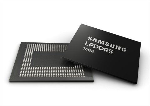
Based on Samsung’s 2nd-generation 10nm-class process technology, the 16GB LPDDR5 mobile DRAM package delivers industry’s highest performance and largest capacity
SEOUL, South Korea — (BUSINESS WIRE) — February 25, 2020 — Samsung Electronics Co., Ltd., a world leader in advanced memory technology, today announced that it has begun mass producing the industry’s first 16-gigabyte (GB) LPDDR5 mobile DRAM package for next-generation premium smartphones. Following mass production of the industry-first 12GB LPDDR5 in July, 2019, the new 16GB advancement will lead the premium mobile memory market with added capacity that enables enhanced 5G and AI features including graphic-rich gaming and smart photography.
This press release features multimedia. View the full release here: https://www.businesswire.com/news/home/20200225005420/en/

16GB LPDDR5 (Graphic: Business Wire)
“Samsung has been committed to bringing memory technologies to the cutting edge in allowing consumers to enjoy amazing experiences through their mobile devices. We are excited to stay true to that commitment with our new, top-of-the-line mobile solution for global device manufacturers,” said Cheol Choi, senior vice president of memory sales & marketing, Samsung Electronics. “With the introduction of a new product lineup based on our next-generation process technology later this year, Samsung will be able to fully address future memory demands from global customers.”
Data transfer rate for the 16GB LPDDR5 comes in at 5,500 megabits per second (Mb/s), approximately 1.3 times faster than the previous mobile memory (LPDDR4X, 4266Mb/s). Compared to an 8GB LPDDR4X package, the new mobile DRAM delivers more than 20-percent energy savings while providing up to twice the capacity.
Samsung’s 16GB LPDDR5 mobile DRAM package consists of eight 12-gigabit (Gb) chips and four 8Gb chips, equipping premium smartphones with twice the DRAM capacity found in many higher-end laptops and gaming PCs today. Along with the blazing-fast performance, the industry’s largest capacity supports dynamic and responsive game play as well as ultra-high-resolution graphics on premium smartphones for highly immersive mobile gaming experiences.
As Samsung continues to expand LPDDR5 mobile DRAM production at its Pyeongtaek site, the company plans to mass-produce 16Gb LPDDR5 products based on third-generation 10nm-class (1z) process technology in the second half of this year, in line with the development of a 6,400Mb/s chipset. Such relentless innovation is expected to well-position Samsung to further solidify its competitive edge in markets such as premium mobile devices, high-end PCs and automotive applications.
###
[Reference] Samsung Mobile DRAM Timeline: Production/Mass Prod.
Date |
Capacity |
Mobile DRAM |
Dec. 2019 |
16GB |
10nm-class 12Gb+8Gb LPDDR5, 5500Mb/s |
Sept. 2019 |
12GB
|
10nm-class 24Gb LPDDR4X, 4266Mb/s |
July 2019 |
12GB |
10nm-class 12Gb LPDDR5, 5500Mb/s |
June 2019 |
6GB |
10nm-class 12Gb LPDDR5, 5500Mb/s |
Feb. 2019 |
12GB |
10nm-class 16Gb LPDDR4X, 4266Mb/s |
July 2018 |
8GB |
10nm-class 16Gb LPDDR4X, 4266Mb/s |
April 2018 |
8GB
|
10nm-class 8Gb LPDDR5, 6400Mb/s |
Sept. 2016 |
8GB |
10nm-class 16Gb LPDDR4X, 4266Mb/s |
Aug. 2015 |
6GB |
20nm 12Gb LPDDR4, 4266Mb/s |
Dec. 2014 |
4GB |
20nm 8Gb LPDDR4, 3200Mb/s |
Sept. 2014 |
3GB |
20nm 6Gb LPDDR3, 2133Mb/s |
Nov. 2013 |
3GB |
20nm-class 6Gb LPDDR3, 2133Mb/s |
July 2013 |
3GB |
20nm-class 4Gb LPDDR3, 2133Mb/s |
April 2013 |
2GB |
20nm-class 4Gb LPDDR3, 2133Mb/s |
Aug. 2012 |
2GB |
30nm-class 4Gb LPDDR3, 1600Mb/s |
2011 |
1/2GB |
30nm-class 4Gb LPDDR2, 1066Mb/s |
| 2010 |
512MB |
40nm-class 2Gb MDDR, 400Mb/s |
| 2009 |
256MB |
50nm-class 1Gb MDDR, 400Mb/s |


