Lattice Extends its Leadership in Delivering Complete, Easy-to-Use Solutions Stacks
- Solutions stack includes customizable reference designs for popular embedded vision use cases such as image sensor bridging, aggregation, splitting, and processing
- Includes support for new Lattice Nexus™ platform and CrossLink-NX™ FPGAs
- Accelerates development of many industrial, automotive, consumer, smart home, and medical applications including machine vision, ADAS, drones, smart doorbells, and endoscopic cameras
HILLSBORO, Ore. — (BUSINESS WIRE) — February 24, 2020 — Lattice Semiconductor Corporation (NASDAQ: LSCC), the low power programmable leader, today extended its position as a global provider of FPGA-based embedded vision solutions with the introduction of the Lattice mVision™ solutions stack. The complete solutions stack includes the modular hardware development boards, design software, embedded vision IP portfolio, and reference designs and demos needed to implement sensor bridging, sensor aggregation, and image processing applications. The Lattice mVision solutions stack accelerates and simplifies the implementation of embedded vision systems such as machine vision, ADAS, drones and AR/VR for the industrial, automotive, consumer, smart home, and medical markets.
This press release features multimedia. View the full release here: https://www.businesswire.com/news/home/20200224005130/en/

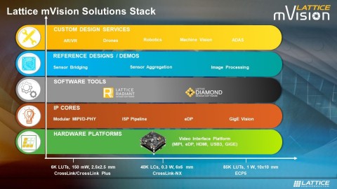
The Lattice mVision™ solutions stack includes the modular hardware development boards, design software, embedded vision IP portfolio, and reference designs and demos needed to quickly and easily develop low power embedded vision systems. (Graphic: Business Wire)
Industry analyst firm Grand View Research forecasts the global machine vision market will reach over $18 billion by 2025.
The Edge AI and Vision Alliance is committed to fostering the adoption of embedded vision in new products. Jeff Bier, the Alliance’s founder, said, “Manufacturing inspection was one of the first markets to widely adopt computer vision. Today, embedded vision is expanding into a wide range of industrial applications, such as automated assembly and inventory. Many of these applications demand small, low cost, low power solutions. I applaud Lattice Semiconductor’s continuing investment in innovation not only in chips, but also in solutions stacks, such as sensAI and mVision, that help developers more easily integrate smart vision capabilities into their product designs.”
“Lattice is committed to delivering complete solutions stacks, such as our multiple award winning sensAI stack, that accelerate the adoption of the disruptive technologies driving growth across multiple end markets,” said Deepak Boppana, Sr. Director of Segment and Solutions Marketing, Lattice Semiconductor. “With our Lattice mVision solutions stack, we bring the ease-of-use benefits of our solutions stacks, as well as the performance, reliability, and power savings made possible by our new Lattice Nexus FPGA development platform, to the embedded vision market.”
Key features of the Lattice mVision solutions stack include the following:
- Video Interface Platform (VIP) - modular hardware development boards with support for a variety of video and I/O interfaces commonly used in embedded vision applications (including MIPI, LVDS, DisplayPort, HDMI, USB, and others). The VIP development boards currently support Lattice FPGAs including CrossLink™, ECP5™ and CrossLink-NX, based on the Lattice Nexus platform.
- Comprehensive IP Library - the Lattice mVision solutions stack includes a wide selection of ready-to-implement IP cores for interfacing to MIPI and LVDS image sensors, image signal processing pipelines, common connectivity standards like USB and Gigabit Ethernet, and display standards such as HDMI, DisplayPort, and GigE Vision.
- Lattice FPGA Design Tools - the stack supports both of Lattice’s easy-to-use FPGA design tools, Lattice Diamond® and Lattice Radiant®. The tools help accelerate and simplify the programming of Lattice FPGAs by automating many common design tasks.
- End-to-end Reference Designs - to further accelerate system development, Lattice mVision offers complete reference designs for common embedded vision applications including sensor bridging, sensor aggregation, and image processing.
- Custom Design Services - for customers requiring assistance to get their embedded vision systems to market, Lattice has developed a network of design service partners who can support a range of customer needs, from developing individual functional design blocks to complete turn-key solutions.
For more information about the Lattice mVision solutions stack, please visit http://www.latticesemi.com/mvision.
About Lattice Semiconductor
Lattice Semiconductor (NASDAQ: LSCC) is the low power programmable leader. We solve customer problems across the network, from the Edge to the Cloud, in the growing communications, computing, industrial, automotive and consumer markets. Our technology, long-standing relationships, and commitment to world-class support lets our customers quickly and easily unleash their innovation to create a smart, secure and connected world.
For more information about Lattice, please visit www.latticesemi.com. You can also follow us via LinkedIn, Twitter, Facebook, YouTube, WeChat, Weibo or Youku.
Lattice Semiconductor Corporation, Lattice Semiconductor (& design) and specific product designations are either registered trademarks or trademarks of Lattice Semiconductor Corporation or its subsidiaries in the United States and/or other countries. The use of the word “partner” does not imply a legal partnership between Lattice and any other entity.
GENERAL NOTICE: Other product names used in this publication are for identification purposes only and may be trademarks of their respective holders.
View source version on businesswire.com: https://www.businesswire.com/news/home/20200224005130/en/
Contact:
MEDIA CONTACTS:
Bob Nelson
Lattice Semiconductor
408-826-6339
Bob.Nelson@latticesemi.com
INVESTOR CONTACT:
Rick Muscha
Lattice Semiconductor
408-826-6000
Rick.Muscha@latticesemi.com


