Silicon-proven, high-bandwidth, low-latency interface extends Cadence high-performance computing IP portfolio for AI/ML, 5G, cloud computing and networking
Highlights
- Silicon proven and prime for customer engagements today
- Supports multi-chip module SoCs on organic substrates
- 40Gbps wire speed delivers up to 1Tbps/mm unidirectional bandwidth
- Achieves better than 10-15 BER without requiring FEC
SAN JOSE, Calif. — (BUSINESS WIRE) — November 13, 2019 — Cadence Design Systems, Inc. (Nasdaq: CDNS) today announced the Cadence® UltraLink™ D2D PHY IP, a high-performance, low-latency PHY for die-to-die connectivity targeted at the AI/ML, 5G, cloud computing and networking market segments. The UltraLink D2D PHY IP is an enabling technology for chiplet and system-in-package (SiP) applications, which empower system-on-chip (SoC) providers to deliver more customized solutions that offer higher performance and yields while also shortening development cycles and reducing costs through greater IP reuse. For more information, please visit www.cadence.com/go/ultralink.
This press release features multimedia. View the full release here: https://www.businesswire.com/news/home/20191113005154/en/

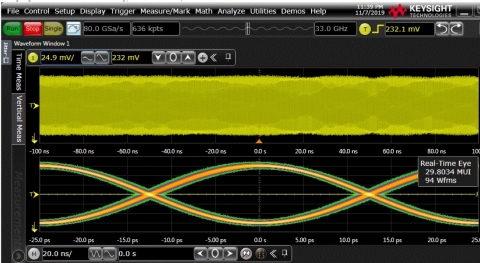
Cadence® Ultralink™ D2D PHY IP 40G Transmit Eye (Graphic: Business Wire)
The UltraLink D2D PHY IP delivers up to 40Gbps wire speed in an NRZ serial interface, providing up to 1Tbps/mm unidirectional bandwidth. The IP includes built-in de-skew and scrambling/de-scrambling logic to enable easy system integration. Its low wire count of 28 data wires for 1Tbps bandwidth enables easier routing and potentially reduces package cost, whereas alternative solutions can require 30% or more wires. While some existing lower speed die-to-die solutions require a silicon interposer to achieve the same bandwidth, the UltraLink D2D PHY IP offers significant cost advantages by supporting multi-chip modules on organic substrates. This IP features latency as low as 5ns round trip from receiver to transmitter, utilizes standard non-return-to zero (NRZ) coding and achieves better than 10-15 bit error rate (BER) without requiring forward error correction (FEC). The UltraLink D2D PHY IP is silicon proven in an advanced 7nm FinFET process.
“As AI and ML in the cloud pose more aggressive computing demands, Cadence continues to invest in design and interface IP that addresses our customers’ rapidly evolving requirements,” said Rishi Chugh, vice president of product marketing, IP Group at Cadence. “Maximizing data transfer with minimal area and power consumption is paramount. The UltraLink D2D PHY IP is the latest addition to our HPC IP portfolio and a critical new technology delivering high bandwidth, low power and latency while extending Cadence’s ongoing investment to support heterogeneous integrated packaging solutions and designs.”
The Cadence UltraLink D2D PHY IP extends Cadence’s broad high-performance computing (HPC) IP portfolio in support of its Intelligent System Design™ strategy, enabling SoC design excellence. It is available now for broad customer engagements.
About Cadence
Cadence enables electronic systems and semiconductor companies to create the innovative end products that are transforming the way people live, work and play. Cadence software, hardware and semiconductor IP are used by customers to deliver products to market faster. The company’s Intelligent System Design strategy helps customers develop differentiated products—from chips to boards to intelligent systems—in mobile, consumer, cloud, data center, automotive, aerospace, IoT, industrial and other market segments. Cadence is listed as one of Fortune Magazine’s 100 Best Companies to Work For. Learn more at cadence.com.
© 2019 Cadence Design Systems, Inc. All rights reserved worldwide. Cadence, the Cadence logo and the other Cadence marks found at www.cadence.com/go/trademarks are trademarks or registered trademarks of Cadence Design Systems, Inc. All other trademarks are the property of their respective owners.
View source version on businesswire.com: https://www.businesswire.com/news/home/20191113005154/en/
Contact:
Cadence Newsroom
408-944-7039
Email Contact


