Highlights:
- Integrated and optimized PHY and digital controller solution enables high-bandwidth and low-latency connectivity for next-generation applications in artificial intelligence (AI), data center, high-performance computing (HPC), enterprise and cloud storage, and 400GbE networking
- PHY supports both PCIe as well Compute Express Link (CXL) connectivity between host processor and workload accelerators for heterogenous computing
- Delivers superior power, performance and area on advanced 7nm FinFET process node
SUNNYVALE, Calif. — (BUSINESS WIRE) — November 12, 2019 — Rambus Inc. (NASDAQ: RMBS), a premier silicon IP and chip provider making data faster and safer, today announced it now offers a comprehensive and optimized interface solution designed for PCI Express (PCIe) 5.0, with backward compatibility to PCIe 4.0, 3.0 and 2.0. The Rambus PCIe 5.0 interface solution includes both PHY and digital controller for easy SoC integration and faster time to market. With the PHY designed for an advanced 7nm process node, the integrated solution offers best-in-class power, performance and area thanks to the industry-proven engineering and signal integrity expertise of Rambus.
This press release features multimedia. View the full release here: https://www.businesswire.com/news/home/20191112005349/en/

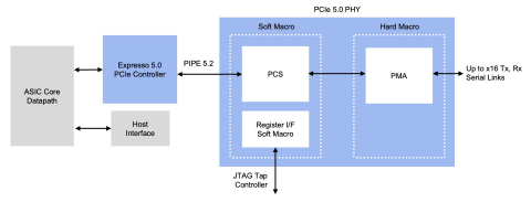
Rambus PCIe 5.0 Interface Architecture (Source: Rambus)
“Our high-speed SerDes and memory interface solutions make possible amazing advancements in performance-intensive applications in AI, data center, HPC, storage and networking,” said Hemant Dhulla, vice president and general manager of IP cores at Rambus. “Now we’ve added PCIe 5 to our industry-leading portfolio of high-speed interface solutions giving chip makers another tool to unleash the power of their designs.”
In addition to the state-of-the-art PHY, the Rambus PCIe 5.0 solution includes a high-performance, digital controller core from recently acquired Northwest Logic. The Rambus PHY and controller are offered as a fully validated and integrated solution, or they can be licensed separately and used with third-party solutions. The entire solution is backed by Rambus design, integration and support services for first-time customer success.
Benefits of Rambus PCIe 5.0 Solution
- Integrated and co-validated PHY and digital controller for complete interface solution
- Built with Rambus’ industry-proven design methodology for long-reach PCIe interfaces
- 32 GT/s bandwidth per lane with 128 GB/s bandwidth in x16 configuration
- Backward compatible to PCIe 4.0, 3.0 and 2.0
- Supports Compute Express Link interconnect
- Advanced multi-tap transceiver and receiver equalization compensate for more than 36dB of insertion loss
- Best-in-class power, performance and area
- Supports performance-intensive applications including AI, data center, HPC, storage and 400GbE networking
Availability and Additional Information
The new Rambus PCIe 5.0 solution is available worldwide in an advanced 7nm FinFET process.
For more information on our complete family of SerDes solutions, please visit rambus.com/serdes.
Follow Rambus:
Company website:
rambus.com
Rambus blog:
rambus.com/blog
Twitter:
@rambusinc
LinkedIn:
www.linkedin.com/company/rambus
Facebook:
www.facebook.com/RambusInc
About Rambus Inc.
Rambus is a premier silicon IP and chip provider that makes data faster and safer. With 30 years of innovation, we continue to develop the foundational technology for all modern computing systems. Leveraging our semiconductor expertise, Rambus solutions speed performance, expand capacity and improve security for today’s most demanding applications. From data center and edge to artificial intelligence and automotive, our interface and security IP, and memory interface chips enable SoC and system designers to deliver their vision of the future. For more information, visit rambus.com.
Source: Rambus Inc.
View source version on businesswire.com: https://www.businesswire.com/news/home/20191112005349/en/
Contact:
Cori Pasinetti
Rambus Corporate Communications
t: (408) 462-8306
Email Contact


