Highlights:
- Rambus GDDR6 Memory PHY has achieved the industry’s highest 18 Gbps performance
- Leading-edge memory PHY IP is four-to-five times faster than current DDR4 solutions
- Offers a complete and optimized memory subsystem of a GDDR6 PHY and a fully-integrated and verified memory controller
- Rambus GDDR6 is well suited for artificial intelligence (AI), machine learning (ML), data center, networking and autonomous driving systems that need higher bandwidth memory
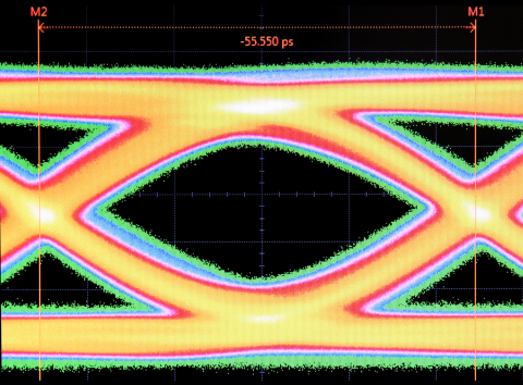
SUNNYVALE, Calif. — (BUSINESS WIRE) — October 30, 2019 — Rambus Inc. (NASDAQ: RMBS), a premier silicon IP and chip provider making data faster and safer, today announced it has achieved industry-leading 18 Gbps performance with the Rambus GDDR6 Memory PHY. Running at the industry’s fastest data rate of 18 Gbps, the Rambus GDDR6 PHY IP delivers peak performance four-to-five times faster than current DDR4 solutions and continues the company’s longstanding tradition of developing leading-edge products. The Rambus GDDR6 PHY pairs with the companion GDDR6 memory controller from the recent acquisition of Northwest Logic to provide a complete and optimized memory subsystem solution.
This press release features multimedia. View the full release here: https://www.businesswire.com/news/home/20191030006031/en/

Rambus GDDR6 18 Gbps Transmit Eye (Graphic: Rambus)
Increased data usage in applications such as AI, ML, data center, networking and automotive systems is driving a need for higher bandwidth memory. The coming introduction of high-bandwidth 5G networks will exacerbate this challenge. Working closely with our memory partners, the Rambus GDDR6 solution gives system designers more options in selecting the memory system that meets both their bandwidth and cost requirements.
“Memory bandwidth poses a significant obstacle for designers working on performance-intensive applications such as AI/ML,” said Hemant Dhulla, vice president and general manager of IP cores at Rambus. “With our GDDR6 18 Gbps memory subsystem, Rambus technology can unleash the power of leading-edge designs with a proven and cost-effective memory architecture.”
Benefits of the Rambus GDDR6 PHY:
- Achieves the industry’s highest speed of up to 18 Gbps, delivering a maximum bandwidth of up to 72 GB/s
- Complete and optimized memory subsystem solution with companion GDDR6 memory controller
- Offers PCB and package design support – allowing customers to quickly and reliably bring their high-speed designs to production
- Provides access to Rambus system and SI/PI experts helping ASIC designers to ensure maximized signal and power integrity for devices and systems
- Features LabStation™ development environment that enables quick system bring-up, characterization and debug
- Supports high-performance applications including networking, data center, ADAS, machine learning and AI
For more information on the Rambus Interface IP, including our PHYs and Controllers, please visit rambus.com/interface-ip.
Follow Rambus:
Company website:
rambus.com
Rambus blog:
rambus.com/blog
Twitter:
@rambusinc
LinkedIn:
www.linkedin.com/company/rambus
Facebook:
www.facebook.com/RambusInc
About Rambus Inc.
Rambus is a premier silicon IP and chip provider that makes data faster and safer. With 30 years of innovation, we continue to develop the foundational technology for all modern computing systems. Leveraging our semiconductor expertise, Rambus solutions speed performance, expand capacity and improve security for today’s most demanding applications. From data center and edge to artificial intelligence and automotive, our interface and security IP, and memory interface chips enable SoC and system designers to deliver their vision of the future. For more information, visit rambus.com.
Source: Rambus Inc.
View source version on businesswire.com: https://www.businesswire.com/news/home/20191030006031/en/
Contact:
Cori Pasinetti
Rambus Corporate Communications
t: (408) 462-8306
Email Contact


