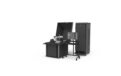
Meridian S expands high sensitivity static OFI capabilities in its industry-leading family of products
HILLSBORO, Ore., Aug. 14, 2019 — (PRNewswire) — With the new Thermo Scientific Meridian S inverted Static Optical Fault Isolation (OFI) solution, semiconductor failure analysis labs can future-proof their operations with a fully scalable solution. Semiconductor failure analysis engineers and technicians can isolate electrical faults that cause semiconductor devices to fail at end-of-line test. These defects, such as metal shorts, opens, and transistor-level leakage, are localized in the failure analysis workflow to troubleshoot process or design failures and increase overall device manufacturing yield. This all-in-one system includes both photon emission and static laser stimulation applications, and is a cost-effective, high-sensitivity solution for localizing electrical failures in semiconductor devices.
The addition of Meridian S also provides semiconductor manufacturers with a reliable static OFI tool that delivers performance. Multiple upgrade paths are available, bringing the industry-leading capabilities of dynamic OFI and high sensitivity emission as customers' lab needs develop.
"Meridian S offers high optical resolution and enhanced sensitivity with a robust upgrade path for future expansion, all in a single tool," said Debbora Ahlgren, senior director, materials and structural analysis, Thermo Fisher Scientific. "The result is a high return on investment and a concrete roadmap as customers increase their OFI capabilities."
Meridian S offers several benefits designed to maximize performance:
- High-sensitivity probing: Meridian S includes FDx with Active Probe, a next-generation Static Laser Simulation (SLS) amplifier for applications such as Optical Beam Induced Resistance Change (OBIRCH) failure analysis.
- Static OFI analysis on a broader range of devices and package types: Meridian S offers both topside probing for flip chip packages and wafer pieces as well as backside probing for conventionally packaged devices.
- Easy-to-use software: Meridian S is optimized to work with the proven Sierra software platform for enhanced ease of use and offers a number of features, including Live Emission mode which allows users to view photon emission signatures emerge in real-time.
- Laser marker option for physical markings of fault locations: Meridian S provides a laser marker option with an accuracy level better than 2 microns.
Meridian S will ship in the fourth quarter of 2019. More information can be found at: Thermofisher.com/MeridianS.
About Thermo Fisher Scientific
Thermo Fisher Scientific is the world leader in serving science, with revenues of more than $24 billion and approximately 70,000 employees globally. Our mission is to enable our customers to make the world healthier, cleaner and safer. We help our customers accelerate life sciences research, solve complex analytical challenges, improve patient diagnostics, deliver medicines to market and increase laboratory productivity. Through our premier brands – Thermo Scientific, Applied Biosystems, Invitrogen, Fisher Scientific and Unity Lab Services – we offer an unmatched combination of innovative technologies, purchasing convenience and comprehensive services. For more information, please visit
thermofisher.com.
Media Contact Information:
Kathy Gill
Thermo Fisher Scientific
+1 971-294-9262
kathy.gill@thermofisher.com

![]() View original content to download multimedia:
http://www.prnewswire.com/news-releases/thermo-fisher-scientific-introduces-scalable-solution-for-optical-fault-isolation-of-semiconductor-devices-300900591.html
View original content to download multimedia:
http://www.prnewswire.com/news-releases/thermo-fisher-scientific-introduces-scalable-solution-for-optical-fault-isolation-of-semiconductor-devices-300900591.html
SOURCE Thermo Fisher Scientific
| Contact: |
| Company Name: Thermo Fisher Scientific
Web: http://www.thermofisher.com |


 Renesas Electronics’ Enhanced RX65N Wi-Fi Connectivity Cloud Kit Simplifies Secure IoT Endpoint Device Connections to Amazon Web Services


