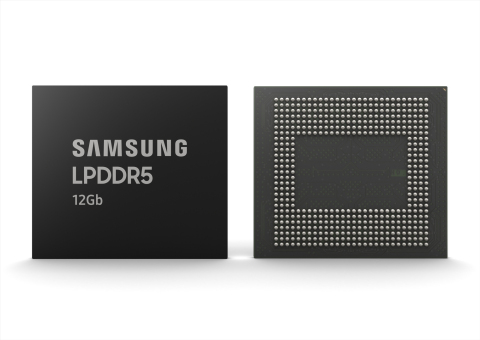
Based on the latest mobile DRAM standard, the new Samsung 12Gb LPDDR5 maximizes the potential of 5G and AI features in future flagships
SEOUL, South Korea — (BUSINESS WIRE) — July 18, 2019 — Samsung Electronics Co., Ltd., the world leader in advanced memory technology, today announced that it has begun mass producing the industry’s first 12-gigabit (Gb) LPDDR5 mobile DRAM, which has been optimized for enabling 5G and AI features in future smartphones. The new mobile memory comes just five months after announcing mass production of the 12GB LPDDR4X, further reinforcing the company’s premium memory lineup. Samsung also plans to start mass producing 12-gigabyte (GB) LPDDR5 packages later this month, each combining eight of the 12Gb chips, in line with growing demand for higher smartphone performance and capacity from premium smartphone manufacturers.
This press release features multimedia. View the full release here: https://www.businesswire.com/news/home/20190718005257/en/

Samsung 12Gb LPDDR5 (Photo: Business Wire)
“With mass production of the 12Gb LPDDR5 built on Samsung’s latest second-generation 10-nanometer (nm) class process, we are thrilled to be supporting the timely launch of 5G flagship smartphones for our customers worldwide,” said Jung-bae Lee, executive vice president of DRAM Product & Technology, Samsung Electronics. “Samsung remains committed to rapidly introducing next-generation mobile memory technologies that deliver greater performance and higher capacity, as we continue to aggressively drive growth of the premium memory market.”
Thanks to its industry-leading speed and power efficiency, Samsung’s new mobile DRAM can enable next-generation flagship smartphones to fully leverage 5G and AI capabilities like ultra-high-definition video recording and machine learning, while greatly extending the battery life.
At a data rate of 5,500 megabits per second (Mb/s), the 12Gb LPDDR5 is approximately 1.3 times faster than previous mobile memory (LPDDR4X, 4266Mb/s) that is found in today’s high-end smartphones. When made into a 12GB package, the LPDDR5 is able to transfer 44GB of data, or about 12 full-HD (3.7GB-sized) movies, in only a second. The new chip also uses up to 30 percent less power than its predecessor by integrating a new circuit design with enhanced clocking, training and low-power feature that ensures stable performance even when operating at a blazingly fast speed.
In order to manage production capacity with more flexibility, Samsung is considering transferring its 12Gb LPDDR5 production to its Pyeongtaek (Korea) campus starting next year, depending on demand from global customers. Following its introduction of the 12Gb LPDDR5 mobile DRAM, Samsung expects to also develop a 16Gb LPDDR5 next year, to solidify its competitive edge in the global memory market.
###
[Reference] Samsung Mobile DRAM Timeline: Production/Mass Prod.
Date |
Capacity |
Mobile DRAM |
July 2019 |
12GB |
10nm-class 12Gb LPDDR5, 5500Mb/s |
June 2019 |
6GB |
10nm-class 12Gb LPDDR5, 5500Mb/s |
Feb. 2019 |
12GB |
10nm-class 16Gb LPDDR4X, 4266Mb/s |
April 2018 |
8GB (development) |
10nm-class 8Gb LPDDR5, 6400Mb/s |
Sept. 2016 |
8GB |
10nm-class 16Gb LPDDR4X, 4266Mb/s |
Aug. 2015 |
6GB |
20nm 12Gb LPDDR4, 4266Mb/s |
Dec. 2014 |
4GB |
20nm 8Gb LPDDR4, 3200Mb/s |
Sept. 2014 |
3GB |
20nm 6Gb LPDDR3, 2133Mb/s |
Nov. 2013 |
3GB |
20nm-class 6Gb LPDDR3, 2133Mb/s |
July 2013 |
3GB |
20nm-class 4Gb LPDDR3, 2133Mb/s |
April 2013 |
2GB |
20nm-class 4Gb LPDDR3, 2133Mb/s |
Aug. 2012 |
2GB |
30nm-class 4Gb LPDDR3, 1600Mb/s |
2011 |
1/2GB |
30nm-class 4Gb LPDDR2, 1066Mb/s |
2010 |
512MB |
40nm-class 2Gb MDDR, 400Mb/s |
2009 |
256MB |
50nm-class 1Gb MDDR, 400Mb/s |
About Samsung Electronics Co., Ltd.
Samsung inspires the world and shapes the future with transformative ideas and technologies. The company is redefining the worlds of TVs, smartphones, wearable devices, tablets, digital appliances, network systems, and memory, system LSI, foundry and LED solutions. For the latest news, please visit the Samsung Newsroom at http://news.samsung.com.
View source version on businesswire.com: https://www.businesswire.com/news/home/20190718005257/en/
Contact:
Ujeong Jahnke
Samsung Semiconductor Europe GmbH
Tel. +49(0)6196-66-3300
Email:
Email Contact


