Multi-Rate PAM-4 SerDes Delivers Industry-Leading PPA Efficiency
SAN JOSE, Calif. — (BUSINESS WIRE) — October 22, 2018 — Cadence Design Systems, Inc. (NASDAQ: CDNS) today unveiled the industry’s first silicon-proven, long-reach 112G SerDes IP in 7nm. The Cadence® 7nm 112G PAM-4 SerDes IP delivers industry-leading power, performance and area (PPA) efficiency required to build high-port density networking products for next-generation cloud-scale and telco datacenters. Cadence has been working closely with early adopter customers, who have expressed strong interest in this innovative technology. Cadence is now ready to engage broadly with customers to enable their next-generation high-performance computing (HPC) ASICs, machine learning accelerators, and switch fabric SoCs. Please visit www.cadence.com/go/112gserdes for more information.
This press release features multimedia. View the full release here: https://www.businesswire.com/news/home/20181022005136/en/

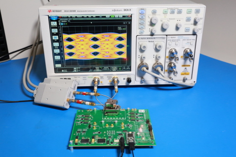
The silicon-proven Cadence 7nm 112G long-reach SerDes is running in Cadence's lab today and available for broad customer adoption now. The test setup includes a demo board featuring the 7nm test chip, which is transmitting a 112G signal with PAM-4 encoding. (Photo: Business Wire)
Escalating mobile data consumption, burgeoning AI and machine learning applications, and emerging 5G communications requirements demand ever-increasing bandwidth, straining the existing cloud datacenter server, storage and networking infrastructure. Early adopters in the high-end cloud datacenter market are now installing 400G Ethernet ports, with 400G Ethernet expected to go mainstream in 2020 as early adopters begin 800G Ethernet deployment. 112G SerDes technology doubles the data rate of 56G SerDes, meeting the exploding high-speed connectivity needs for emerging data-intensive applications such as machine learning and neural networks.
Based on technology gained from Cadence’s 2017 acquisition of nusemi inc, the long-reach 112G SerDes supports backplane, copper and optical connections. Key benefits include:
- Unique firmware-controlled adaptive power design provides optimal power and performance tradeoffs and more efficient system designs based on platform requirements
- DSP-based architecture provides superior data recovery for lossy and noisy channels
- Extended reach capability enables customers to use lower cost PCBs and achieve greater flexibility in PCB and system design
- Multi-rate support, including 112/56Gbps PAM-4 (four-level pulse amplitude modulation) and 56/28/10Gbps NRZ (non-return-to-zero) data rate, provides backward compatibility with legacy equipment operating at lower speeds
- Fully autonomous startup and adaptation, as well as an integrated BIST (built-in self-test) capable of producing and checking PRBS (pseudo random binary sequence), are supported to enhance IP ease of use
“The 112G SerDes is a new and critical enabling technology that allows the industry to build out the next-generation 100G, 400G and 800G Ethernet cloud infrastructure more rapidly and cost effectively,” said Lip-Bu Tan, chief executive officer of Cadence. “Our silicon-proven 112G long-reach multi-rate SerDes IP places Cadence at the forefront of high-performance computing system design enablement. By enabling 100Gb/sec per lane, Cadence’s solution reduces the lane count, heat dissipation and cost required to build the next generation of hyperscale infrastructure.”
Availability
Early adopter customers have already begun to design the new SerDes into their SoCs, and Cadence is available for broad customer engagements now.
About Cadence
Cadence enables electronic systems and semiconductor companies to create the innovative end products that are transforming the way people live, work and play. Cadence software, hardware and semiconductor IP are used by customers to deliver products to market faster. The company’s System Design Enablement strategy helps customers develop differentiated products—from chips to boards to systems—in mobile, consumer, cloud datacenter, automotive, aerospace, IoT, industrial and other market segments. Cadence is listed as one of Fortune Magazine’s 100 Best Companies to Work For. Learn more at cadence.com.
© 2018 Cadence Design Systems, Inc. All rights reserved worldwide. Cadence, the Cadence logo and the other Cadence marks found at www.cadence.com/go/trademarks are trademarks or registered trademarks of Cadence Design Systems, Inc. All other trademarks are the property of their respective owners.
View source version on businesswire.com: https://www.businesswire.com/news/home/20181022005136/en/
Contact:
Cadence Newsroom
408-944-7039
Email Contact


