Boosts Single-Chip Memory Capacity to Highest Level yet Achieved
SAN JOSE, Calif. — (BUSINESS WIRE) — July 19, 2018 — Toshiba Memory America, Inc. (TMA), the U.S.-based subsidiary of Toshiba Memory Corporation, today announced the development of a prototype sample of 96-layer BiCS FLASHTM, its proprietary three-dimensional (3D) flash memory, with 4-bit-per-cell (quad level cell, QLC) technology. With this milestone achievement, Toshiba demonstrates its technology leadership in the storage market by delivering technology that boosts single-chip memory capacity to the highest level yet achieved1.
This press release features multimedia. View the full release here: https://www.businesswire.com/news/home/20180719005984/en/

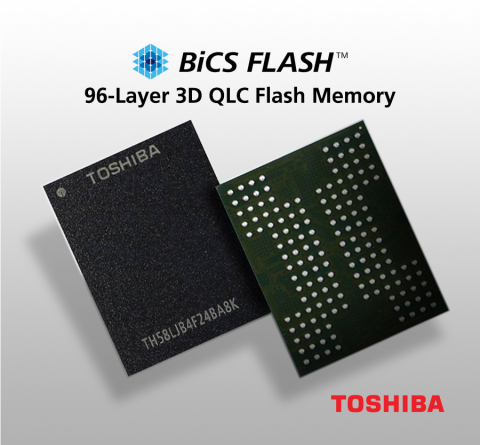
Toshiba Memory's 96-layer BiCS FLASH 3D flash memory boosts single-chip memory capacity to the highest level yet achieved. (Graphic: Business Wire)
Toshiba’s new QLC BiCS FLASH significantly expands capacity by pushing the bit count for data per memory cell from three to four. The new product achieves the industry's maximum capacity of 1.33 terabits2 for a single chip, and a 16-die stacked architecture in a single package realizes an unparalleled capacity of 2.66 terabytes.
The number of applications needing huge amounts of storage continues to grow, fed by the enormous volumes of data being generated that need to be accessed and analyzed in real time. Social media, SSDs, edge computing, enterprise applications and the rapidly expanding data center storage market are all areas in which larger capacity storage is required – to name just a few. With the introduction of 96-layer QLC technology, Toshiba Memory enables the development of products that keep pace with the fast-moving storage market.
QLC technology has long been a part of Toshiba’s roadmap strategy for high-density, smaller chip size flash memory solutions: the company was the first to publicly discuss QLC technology (at the 2016 Flash Memory Summit) and one of the first to develop a 3D flash memory device that uses it.
“We were among the first in the industry to envision and prepare for the successful migration of SLC technology to MLC, from MLC to TLC, and now from TLC to QLC,” noted Scott Nelson, senior vice president of TMA’s Memory Business Unit. “This technology evolution has made increasingly dense packaging options available, and QLC will have a game-changing impact across many different markets.”
Samples of Toshiba’s groundbreaking QLC device will begin shipping in early September to SSD and SSD controller vendors for evaluation and development purposes. Mass production is expected to begin in 2019. Additionally, a packaged prototype will be showcased at the 2018 Flash Memory Summit, taking place from August 6-9 in Santa Clara, California. For more information, please visit www.Toshiba.com/TMA.
Notes:
[1] Source: Toshiba Memory Corporation, as of July
19, 2018.
[2] Definition of capacity: Toshiba Memory Corporation
defines a gigabyte (GB) as 1,000,000,000 bytes. A computer operating
system, however, reports storage capacity using powers of 2 for the
definition of 1GB = 2^30 bytes = 1,073,741,824 bytes and therefore shows
less storage capacity. Available storage capacity (including examples of
various media files) will vary based on file size, formatting, settings,
software and operating system, such as Microsoft Operating System and/or
pre-installed software applications, or media content. Actual formatted
capacity may vary.
About Toshiba Memory America, Inc.
Toshiba Memory America, Inc. (TMA) is the U.S.-based subsidiary of Toshiba Memory Corporation, a leading worldwide supplier of flash memory and solid state drives (SSDs). From the invention of flash memory to today’s breakthrough 96-layer BiCS FLASH™ 3D technology, Toshiba continues to lead innovation and move the industry forward. For more information on TMA, please visit www.toshiba.com/tma and follow the company on LinkedIn, Twitter ( @Toshiba_Memory) and Facebook.
© 2018 Toshiba Memory America, Inc. All rights reserved. Information in this press release, including product pricing and specifications, content of services, and contact information is current and believed to be accurate on the date of the announcement, but is subject to change without prior notice. Technical and application information contained here is subject to the most recent applicable Toshiba product specifications.
View source version on businesswire.com: https://www.businesswire.com/news/home/20180719005984/en/
Contact:
COMPANY CONTACT:
Toshiba Memory America, Inc.
Rebecca
Bueno, 949-737-7321
Email Contact
or
MEDIA
CONTACT:
Lages & Associates
Dena Jacobson, 949-453-8080
Email Contact


