TOKYO — (BUSINESS WIRE) — November 28, 2017 — Toshiba Memory Corporation, the world leader in memory solutions, has today started sampling Universal Flash Storage (UFS) devices[1] utilizing Toshiba Memory Corporation’s cutting-edge 64-layer, BiCS FLASH™ 3D flash memory. [2] The new UFS devices meet performance demands for applications that require high-speed read/write performance and low power consumption, including mobile devices such as smartphones and tablets, and augmented and virtual reality systems.
This press release features multimedia. View the full release here: http://www.businesswire.com/news/home/20171128006597/en/

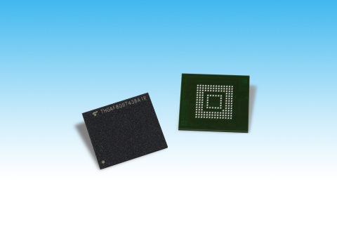
Toshiba Memory Corporation: UFS devices utilizing 64-layer, BiCS FLASH(TM) 3D flash memory (Photo: Business Wire)
The new line-up will be available in four capacities: 32GB, 64GB, 128GB and 256GB. [3] All of the devices integrate flash memory and a controller in a single, JEDEC-standard 11.5 x 13mm package. The controller performs error correction, wear leveling, logical-to-physical address translation and bad-block management, allowing users to simplify system development.
All four devices are compliant with JEDEC UFS Ver2.1, including HS-GEAR3, which has a theoretical interface speed of up to 5.8Gbps per lane (x2 lanes = 11.6Gbps) while also suppressing any increase in power consumption. Sequential read and write performance[4] of the 64GB device are 900MB/s and 180MB/s, while the random read and write performance are around 200% and 185% better, respectively, than those of previous generation devices[5]. Due to its serial interface, UFS supports full duplexing, which enables both concurrent reading and writing between the host processor and UFS device.
* Company names, product names, and service names mentioned herein may be trademarks of their respective companies.
Notes
[1] Universal Flash Storage (UFS) is a product category for a
class of embedded memory products built to the JEDEC UFS standard
specification.
[2] Sample shipments of the 64GB device will start
today with the rest of the line-up to gradually follow after December.
[3]
Product density is identified based on the density of memory chip(s)
within the Product, not the amount of memory capacity available for data
storage by the end user. Consumer-usable capacity will be less due to
overhead data areas, formatting, bad blocks, and other constraints, and
may also vary based on the host device and application. For details,
please refer to applicable product specifications.
[4] Read and
write speeds are calculated as 1MB/s = 1,000,000bytes/s. Actual read and
write speed may vary depending on the device, read and write conditions,
and file size.
[5] Toshiba Memory Corporation’s previous generation
64GB device “THGAF4G9N4LBAIR”
Customer Inquiries:
Memory Marketing Division
Tel:
+81-3-3457-3461
https://toshiba.semicon-storage.com/ap-en/contact.html
Information in this document, including product prices and specifications, content of services and contact information, is correct on the date of the announcement but is subject to change without prior notice.
View source version on businesswire.com: http://www.businesswire.com/news/home/20171128006597/en/
Contact:
Media Inquiries:
Toshiba Memory Corporation
Koji Takahata,
+81-3-3457-3822
Sales Strategic Planning Division
Email Contact


