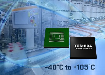
e-MMC Version 5.1-Compliant; Feature Enhanced Operational Temperature Range of +105°C
IRVINE, Calif., Jan. 10, 2017 — (PRNewswire) — Toshiba America Electronic Components, Inc. (TAEC)* today announced the launch of its JEDEC®[1] e-MMCTM Version 5.1[2]-compliant embedded NAND flash memory products that feature an enhanced operational temperature range of -40°C to +105°C. The new parts integrate NAND chips fabricated with 15nm process technology and are well suited to industrial applications including PLC[3] and CoMs[4], as well as factory automation equipment. The new lineup includes densities of 8 gigabyte (GB), 16GB, 32GB and 64GB.
The number of consumer and industrial applications that utilize e-MMC for high-density, low power embedded memory continues to grow. As a result, the variety of e-MMC solutions needed to address these diverse requirements has expanded, as has the need for products with extended temperature ranges. Toshiba is meeting the demand for high temperature solutions by adding to its lineup of high-performance, high-density e-MMC products.
As with Toshiba's existing e-MMC lineup, the new products integrate NAND chips with a controller to manage basic control functions for NAND applications in a single package. By supporting operational temperatures of +105°C, the new e-MMC devices give developers a mass storage solution for industrial applications in high temperature environments.
New Product Lineup
|
Product Name |
Capacity |
Category |
Package |
|
THGBMHG6C1LBAU6 |
8GB |
Upper Extended
|
11.5x13x0.8mm |
|
THGBMHG7C2LBAU7 |
16GB |
11.5x13x1.0mm | |
|
THGBMHG8C4LBAU7 |
32GB |
11.5x13x1.0mm | |
|
THGBMHG9C8LBAU8 |
64GB |
11.5x13x1.2mm |
Key Features
- Handles essential functions, including writing block management, error correction and driver software.
- Simplifies system development, allowing manufacturers to minimize costs and speed up time to market for new and upgraded products.
- Enhances usability with new features[5] standardized in JEDECe-MMC Version 5.1, including BKOPS control, cache barrier, cache flushing report, large RPMB write and command queuing.
- Supports operational temperature range of -40°C to +105°C.
Key Specifications
|
Interface |
JEDECe-MMC V5.1 standard
|
|
Capacity |
8GB, 16GB, 32GB, 64GB |
|
Power Supply
|
2.7-3.6V (Memory core)
|
|
Bus Width |
x1, x4, x8 |
|
Temperature
|
-40oC to +105oC |
|
Package |
153Ball FBGA 11.5mm x 13.0mm |
Sample shipments begin today, with mass production scheduled for March 2017. For more information, please visit toshiba.com/technologymoves, read the TAEC Memory Blog and follow the company on Facebook and Twitter.
Notes
[1] JEDEC is a registered trademark of JEDEC Solid State Technology Association.
[2] e-MMC is a product category for a class of embedded memory products built to the JEDEC e-MMC Standard specification and is a trademark of the JEDEC Solid State Technology Association. The latest JEDEC e-MMC Version 5.1 specification was officially issued by JEDEC on February 24, 2015.
[3] Programmable Logic Controller.
[4] Computer on Modules.
[5] "BKOPS control" is a function where the host allows the device to perform background operation when the device is idle. "Cache Barrier" is a function that controls when cache data is written to the memory chip. "Cache Flushing Report" is a function that informs the host if the device's flushing policy is FIFO (First In First Out) or not. "Large RPMB write" is a function that enhances the data size that can be written to the RPMB area to 8KB.
"Command Queuing" feature allows users to process multiple tasks generated by the user's issue of multiple commands, in the order of the user's preference, by initially storing the tasks in a waiting queue. It improves random read performance speed by approximately 30% at maximum according to Toshiba survey.
*The products are labeled based on the memory chip(s) it contains, not the amount of memory capacity available for data storage by the end user. Part of the capacity is reserved for device management. Please refer to the data sheet or your local Toshiba sales representative. (For purposes of measuring memory capacity in this context, 1GB = 1,073,741,824 bytes).
Product density is identified based on the density of memory chip(s) within the Product, not the amount of memory capacity available for data storage by the end user. Consumer-usable capacity will be less due to overhead data areas, formatting, bad blocks, and other constraints, and may also vary based on the host device and application. For details, please refer to applicable product specifications.
*About TAEC
Through proven commitment, lasting relationships and advanced, reliable electronic components, Toshiba enables its customers to create market-leading designs. Toshiba is the heartbeat within product breakthroughs from OEMs, ODMs, CMs, VARs, distributors and fabless chip companies worldwide. A committed electronic components leader, Toshiba designs and manufactures high-quality flash memory-based storage solutions, solid state drives (SSDs), hard disk drives (HDDs), solid state hybrid drives (SSHDs), discrete devices, custom SoCs/ASICs, imaging products, microcontrollers, wireless components, mobile peripheral devices, advanced materials and medical tubes that make possible today's leading smartphones, tablets, cameras, medical devices, automotive electronics, industrial applications, enterprise solutions and more.


