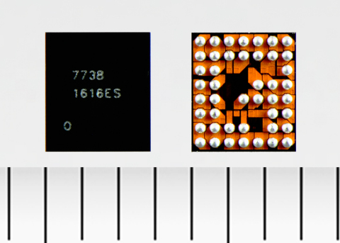
TOKYO — (BUSINESS WIRE) — December 14, 2016 — Toshiba Corporation's (TOKYO:6502) Storage & Electronic Devices Solutions Company today launched "TC7738WBG," a multi-function system power IC suited for the power supply of SSD components, such as the SoC core block, IO blocks, NAND flash memory, DRAM, and various sensors. Sample shipments start today with mass production shipments scheduled for the end of January next year.
This Smart News Release features multimedia. View the full release here: http://www.businesswire.com/news/home/20161214006362/en/

Toshiba: a multi-function system power IC "TC7738WBG" suitable for a power supply of the SSD components such as an SoC core block, IO blocks, NAND flash memory, DRAM, and various sensors. (Photo: Business Wire)
The “TC7738WBG” is a multi-output power supply IC that incorporates a 6-channel DC-DC converter, a 2-channel power supply and an input protection switch. In systems that use SSD, the voltage differs depending on the interface or application. The new IC allows the input voltage mode setting and output voltage of each channel to be changed simply by changing pin settings, enabling use in numerous systems.
In a typical system, the power supply input line is generally protected by a dedicated IC. Toshiba’s new power IC incorporates this same function as an input protection switch with low-input voltage, over-voltage detection, and a soft start function to prevent inrush current.
The new IC has a function to control the DC-DC converter by automatic switching of Pulse Width Modulation (PWM) or Pulse Frequency Modulation (PFM) operations according to the output load, and realizes highly efficient characteristic in both heavy and light load systems. This allows the IC to support various applications, including portable devices.
Applications
SSD, portable devices,
etc.
Main Features of New Product
- Built-in input protection switch
- Supports both 3.3V and 5V systems by changing pin settings
- Buck DC-DC converters (6ch) + LDO (2ch) + load switch (1ch)
- Efficiency control during light load conditions (by switching PWM/PFM operation)
- Compact package (WCSP45; 3.31mm x 2.91mm)
|
Main Specifications |
||||||||||||||
|
Part number |
TC7738WBG | |||||||||||||
|
Control I/F |
I2C | |||||||||||||
|
Input voltage |
3.3V input setting: 2.9 to 3.6V; 5V input setting: 4 to 5.5V | |||||||||||||
|
Package |
WCSP45 (Size: 3.31 mm x 2.91 mm; Pin pitch: 0.4mm) | |||||||||||||
|
DC-DC |
|
Setting 1 |
Setting 2 |
Output
|
||||||||||
|
|
3.3V mode |
5V mode |
3.3V mode |
5V mode |
||||||||||
|
ch1 |
By-pass
|
2.5V |
By-pass
|
2.5V |
4A |
|||||||||
|
ch2 |
1.35V |
1.2V |
1A |
|||||||||||
|
ch3 |
1.8V |
1.8V |
2A |
|||||||||||
|
ch4 |
1.0V |
1.8V |
1A |
|||||||||||
|
ch5 |
1.0V |
0.9V |
1A |
|||||||||||
|
ch6 |
1.0V |
0.9V |
3.5A |
|||||||||||
|
Series power
|
Setting |
Setting 1 |
Setting 2 |
Output
|
||||||||||
|
3.3V mode |
5V mode |
3.3V mode |
5V mode |
|||||||||||
|
LDO1 |
2.5V |
1.8V |
0.3A |
|||||||||||
|
LDO2 |
Bypass
|
2.5V |
Bypass
|
3.3V |
0.3A |
|||||||||
|
Input
|
ON resistance: 20 mΩ (Typ.)
|
|||||||||||||
|
Abnormality
|
Output over-voltage detection, output undervoltage detection,
|
|||||||||||||
|
Mass
|
End of January 2017 (scheduled) | |||||||||||||


