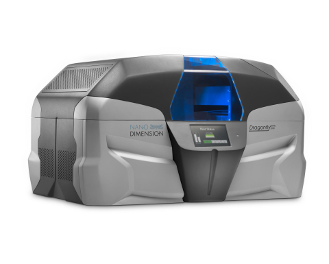
DragonFly 2020 3D Printer being Demonstrated at Printed Electronics USA 2015 Saves Time and Money by Creating Functional PCB Prototypes In-House
SANTA CLARA, Calif. — (BUSINESS WIRE) — November 18, 2015 — PRINTED ELECTRONICS USA -- Nano Dimension Ltd. (TASE: NNDM, OTCQX: NNDMY) today revealed the world’s first desktop-sized 3D printer designed specifically for the production of professional multilayer printed circuit boards (PCBs). The DragonFly 2020 3D Printer, being demonstrated in the US for the first time at the Printed Electronics USA 2015 conference (Booth F09), will allow users to build functional, multilayer circuit board prototypes in-house –in a matter of hours.
This Smart News Release features multimedia. View the full release here: http://www.businesswire.com/news/home/20151118005101/en/

DragonFly 2020: The World's First 3D Printer for Professional Multilayer PCBs (Photo Credit: Yoram Reshef)
The capability of rapidly producing functional multilayer PCB prototypes using 3D printing is new to the printed electronics design and manufacturing industry. The current standard subtractive manufacturing of PCBs is a multi-stage, labor- and material-intensive process, and is so costly and time consuming that electronics designers requiring prototypes resort to outsourcing. Nano Dimension’s 3D printer can print a complete multilayer PCB, including all interconnections between layers, using its revolutionary inkjet printer and highly conductive nano-inks. Sophisticated proprietary software accepts industry standard Gerber design files and manages the precise print process. In addition, the DragonFly 2020 3D Printer gives users the option of testing on-the-fly, testing a range of designs and exploring new circuit geometries.
The DragonFly 2020 3D Printer is a three-axis inkjet printer; its benefits and attributes include:
- On-site ultra-rapid prototyping of professional multilayer prototype PCBs including interconnections and through-holes.
- Reduced PCB design and test cycles, from months or weeks to days.
- Minimize costs and inexpensively evaluate design alternatives and creative ideas.
- Security of IP, sensitive design information stays in-house.
- A greener alternative to standard PCB production since it is a cleaner process with no waste.
- Compact, office-friendly 3D printer.
“For designers and engineers looking for ultra-rapid prototyping of PCBs, our 3D printer is a significant leap forward. The DragonFly 3D Printer eliminates the frustration they face when they reach the prototyping and testing stage,” said Simon Fried, Chief Marketing Officer at Nano Dimension. “Moving their work from design to a prototype at an off-site printing facility might take weeks for the PCB to be ordered, produced and shipped. If further iterations are needed, it’s back to the prototyping house for another cycle. In today’s competitive electronics markets, unforeseeable and costly delays during PCB development can significantly slow time-to-market. That’s the development risk and bottleneck that we’re eliminating with the DragonFly 2020.”
At Printed Electronics USA, Nano Dimension is also exhibiting its AgCite line of conductive silver nanoparticle inks for inkjet deposition and 3D printed PCB prototype samples. In addition, Nano Dimension’s CMO Simon Fried will give a presentation on “What happens when 3D printing and conductive inks converge?”
The DragonFly 2020 3D Printer is targeted for commercial availability during the second half of 2016. The AgCite conductive inks are available today.
About Nano Dimension
Nano Dimension, founded in 2012, focuses on the development of advanced 3D printed electronics systems. Nano Dimension's unique products combine three advanced technologies: 3D inkjet, 3D software and nanomaterials. The company's primary products include the first 3D printer dedicated to printing multilayer PCBs (printed circuit boards) and advanced nanotechnology-based conductive and dielectric inks.
Nano Dimension trades on OTCQX® Best Market in the U.S. and on the TASE in Israel. U.S. investors can find current financial disclosure and Real-Time Level 2 quotes for Nano Dimension on http://www.otcmarkets.com/stock/NNDMY.
Forward Looking Statement
This press
release contains forward-looking statements. Words such as "expects,"
"anticipates," "intends," "plans," "believes," "seeks," "estimates" and
similar expressions or variations of such words are intended to identify
forward-looking statements. These statements are only predictions based
on Nano Dimension’s current expectations and projections about future
events. There are important factors that could cause Nano' Dimension’s
actual results, level of activity, performance or achievements to differ
materially from the results, level of activity, performance or
achievements expressed or implied by the forward-looking statements.
Those factors include, but are not limited to the impact of general
economic conditions, competitive products, product development risk,
product demand and market acceptance risks, reliance on key strategic
alliances or fluctuations in operating results. Except as otherwise
required by law, Nano Dimension undertakes no obligation to publicly
release any revisions to these forward-looking statements to reflect
events or circumstances after the date hereof or to reflect the
occurrence of unanticipated events.


