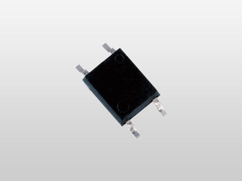
TOKYO — (BUSINESS WIRE) — April 25, 2014 — Toshiba Corporation’s (TOKYO:6502) Semiconductor & Storage Products Company today announced the launch of small-size SO6 package photovoltaic couplers. Mass production of the new products, “TLP3905” and “TLP3906”, starts today.

Toshiba: SO6 Package Photovoltaic Coupler (Photo: Business Wire)
The structure of a photovoltaic coupler is a photorelay without a MOSFET chip. Users can create an isolated relay by combining the photovoltaic coupler with the external MOSFET of their choice. This makes it possible to realize larger voltage and current exceeding the capabilities of existing photorelay products.
The new products, “TLP3905” and “TLP3906”, while maintaining the fundamental performance of Toshiba’s current products, “TLP190B” and “TLP191B”, expand on application areas by upgrading the operating temperature up to 125 degrees Celsius (max) and the isolation voltage up to 3750Vrms (min). Also, “TLP3906” integrates a control circuit for releasing the MOSFET gate charge, realizing a much faster turn-off speed; approximately triple that of “TLP3905”. Additionally, “TLP3906” guarantees an LED trigger current to ensure VOC (min)*, making it easier to lower power dissipation of LED current. The new products are suitable for line switches in tester applications or high current control in PLC applications.
*VOC: Open circuit voltage
|
Main Specifications of New Products |
||||||||||||||
| Product | Current Products | New Products | ||||||||||||
| TLP190B | TLP191B | TLP3905 | TLP3906 | |||||||||||
| Package | MFSOP6 | SO6(4pin) | ||||||||||||
| Function |
Without
|
With
|
Without
|
With
|
||||||||||
| Term | Unit | |||||||||||||
|
Open Circuit Voltage
|
VOC | V | 7 | 7 | 7 | 7 | ||||||||
| Short Circuit Current(min) | I SC | µA | 12 | 12 | 12 | 12 | ||||||||
|
Trigger LED Current
|
I FT | mA | - | - | - | 3 | ||||||||
|
Isolation Voltage
|
BVs | Vrms | 2500 | 3750 | ||||||||||
| Switching |
Turn On
|
t ON | ms | 0.2 | 0.2 | 0.3 | 0.2 | |||||||
|
Turn Off
|
t OFF | ms | 1 | 3 | 1 | 0.3 | ||||||||
| Condition |
I F =20mA,
|
I F =20mA
|
I F =10mA,
|
I F =10mA,
|
||||||||||
| Safety Standard | UL, cUL |
UL, cUL,
|
||||||||||||


