|
10.2 A 4-bit Multiplier
Chapter start Previous
page Next page
10.2 A 4-bit Multiplier
This section presents
a more complex VHDL example to motivate the study of the syntax and semantics
of VHDL in the rest of this chapter.
10.2.1 An 8-bit Adder
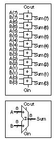
Table 10.1 shows
a VHDL model for the full adder that we described in Section 2.6, "Datapath
Logic Cells." Table 10.2 shows a VHDL model for an 8-bit ripple-carry
adder that uses eight instances of the full adder.
TABLE 10.1 A
full adder. |
entity Full_Adder is
	generic (TS : TIME := 0.11 ns; TC : TIME := 0.1 ns);
	port (X, Y, Cin: in BIT; Cout, Sum: out  BIT);
end Full_Adder;
architecture Behave of Full_Adder is
begin
Sum  <= X xor Y xor Cin after TS;
Cout <= (X and Y) or (X and Cin) or (Y and Cin) after TC;
end;
|

|
Timing:
TS (Input to Sum) = 0.1
1 ns
TC (Input to Cout) =
0.1 ns
|
TABLE 10.2 An
8-bit ripple-carry adder. |
entity Adder8 is
	port (A, B: in BIT_VECTOR(7 downto 0);
	Cin: in BIT; Cout: out BIT;
	Sum: out BIT_VECTOR(7 downto 0));
end Adder8;
architecture Structure of Adder8 is
component Full_Adder
port (X, Y, Cin: in BIT; Cout, Sum: out BIT);
end component;
signal C: BIT_VECTOR(7 downto 0);
begin
Stages: for i in 7 downto 0 generate
	LowBit: if i = 0 generate
	FA:Full_Adder port map (A(0),B(0),Cin,C(0),Sum(0));
	end generate;
	OtherBits: if i /= 0 generate
	FA:Full_Adder port map
		(A(i),B(i),C(i-1),C(i),Sum(i));
	end generate;
end generate;
Cout <= C(7);
end;
|

|
10.2.2 A Register Accumulator
Table 10.3 shows
a VHDL model for a positive-edge-triggered D flip-flop with an active-high
asynchronous clear. Table 10.4 shows an 8-bit register that uses this
D flip-flop model (this model only provides the Q output from
the register and leaves the QN flip-flop outputs unconnected).
TABLE 10.3 Positive-edge-triggered
D flip-flop with asynchronous clear. |
entity DFFClr is
	generic(TRQ : TIME := 2 ns; TCQ : TIME := 2 ns);
	port (CLR, CLK, D : in BIT; Q, QB : out BIT);
end;
architecture Behave of DFFClr is
signal Qi : BIT;
begin QB <= not Qi; Q <= Qi;
process (CLR, CLK) begin
	if CLR = '1' then Qi <= '0' after TRQ;
	elsif CLK'EVENT and CLK = '1'
		then Qi <= D after TCQ;
	end if;
end process;
end;
|

|
Timing:
TRQ (CLR
to Q/QN) = 2 ns
TCQ (CLK
to Q/QN) = 2 ns
|
TABLE 10.4 An
8-bit register. |
entity Register8 is
	port (D : in BIT_VECTOR(7 downto 0);
	Clk, Clr: in BIT ; Q : out BIT_VECTOR(7 downto 0));
end;
architecture Structure of Register8 is
	component DFFClr
		port (Clr, Clk, D : in BIT; Q, QB : out BIT);
	end component;
	begin
		STAGES: for i in 7 downto 0 generate
		FF: DFFClr port map (Clr, Clk, D(i), Q(i), open);
		end generate;
end;
|

|
8-bit register. Uses
DFFClr positive edge-triggered
flip-flop model. |
Table 10.5 shows a model
for a datapath multiplexer that consists of eight 2:1 multiplexers with
a common select input (this select signal would normally be a control signal
in a datapath). The multiplier will use the register and multiplexer components
to implement a register accumulator.
TABLE 10.5 An
8-bit multiplexer. |
entity Mux8 is
	generic (TPD : TIME := 1 ns);
	port (A, B : in BIT_VECTOR (7 downto 0);
	Sel : in BIT := '0'; Y : out BIT_VECTOR (7 downto 0));
end;
architecture Behave of Mux8 is
begin
	 Y <= A after TPD when Sel = '1' else B after TPD;
end;
|

|
Eight 2:1 MUXs with
single select input.
Timing:
TPD (input
to Y) = 1 ns
|
10.2.3 Zero Detector
Table 10.6 shows
a model for a variable-width zero detector that accepts a bus of any width
and will produce a single-bit output of '1' if all input bits
are zero.
TABLE 10.6 A
zero detector. |
entity AllZero is
	generic (TPD : TIME := 1 ns);
	port (X : BIT_VECTOR; F : out BIT );
end;
architecture Behave of AllZero is
begin process (X) begin F <= '1' after TPD;
	 for j in X'RANGE loop
		if X(j) = '1' then F <= '0' after TPD; end if;
	 end loop;
end process;
end;
|

|
Variable-width zero detector.
Timing:
TPD (X to
F) = 1 ns
|
10.2.4 A Shift Register
Table 10.7 shows
a variable-width shift register that shifts (left or right under input control,
DIR ) on the positive edge of the clock, CLK ,
gated by a shift enable, SH . The parallel load, LD
, is synchronous and aligns the input LSB to the LSB of the output, filling
unused MSBs with zero. Bits vacated during shifts are zero filled. The clear,
CLR , is asynchronous.
TABLE 10.7 A
variable-width shift register. |
entity ShiftN is
	generic (TCQ : TIME := 0.3 ns; TLQ : TIME := 0.5 ns;
		TSQ : TIME := 0.7 ns);
	port(CLK, CLR, LD, SH, DIR: in BIT;
		D: in BIT_VECTOR; Q: out BIT_VECTOR);
	begin assert (D'LENGTH <= Q'LENGTH)
		report "D wider than output Q" severity Failure;
end ShiftN;
architecture Behave of ShiftN is
	begin Shift: process (CLR, CLK)
	subtype InB  is NATURAL range D'LENGTH-1 downto 0;
	subtype OutB is NATURAL range Q'LENGTH-1 downto 0;
	variable St: BIT_VECTOR(OutB);
	begin
		if CLR = '1' then
			St := (others => '0'); Q <= St after TCQ;
		elsif CLK'EVENT and CLK='1' then
			if LD = '1' then
				St := (others => '0');
				St(InB) := D;
				Q <= St after TLQ;
			elsif SH = '1' then
				case DIR is
				when '0' => St := '0' & St(St'LEFT downto 1);
				when '1' => St := St(St'LEFT-1 downto 0) & '0';
				end case;
				Q <= St after TSQ;
			end if;
		end if;
	end process;
end;
|

|
CLK Clock
CLR Clear, active high
LD Load, active high
SH Shift, active high
DIR Direction, 1 = left
D Data in
Q Data out
Variable-width shift
register. Input width must be less than output width. Output is left-shifted
or right-shifted under control of DIR. Unused MSBs are zero-padded during
load. Clear is asynchronous. Load is synchronous.
Timing:
TCQ (CLR
to Q) = 0.3 ns
TLQ (LD
to Q) = 0.5 ns
TSQ (SH
to Q) = 0. 7 ns
|
10.2.5 A State Machine
To multiply two binary numbers A
and B , we can use the following algorithm:
If the LSB of A is '1',
then add B into an accumulator.
Shift A one bit to the right and B
one bit to the left.
Stop when all bits of A are zero.
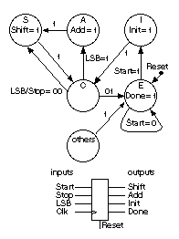
Table 10.8 shows the VHDL model for a Moore (outputs
depend only on the state) finite-state machine for the multiplier, together
with its state diagram.
TABLE 10.8 A
Moore state machine for the multiplier. |
entity SM_1 is
	generic (TPD : TIME := 1 ns);
	port(Start, Clk, LSB, Stop, Reset: in BIT;
	Init, Shift, Add, Done : out BIT);
end;
architecture Moore of SM_1 is
type STATETYPE is (I, C, A, S, E);
signal State: STATETYPE;
begin
Init <= '1' after TPD when State = I
	else '0' after TPD;
Add  <= '1' after TPD when State = A
	else '0' after TPD;
Shift <= '1' after TPD when State = S
	else '0' after TPD;
Done <= '1' after TPD when State = E
	else '0' after TPD;
process (CLK, Reset) begin
	if Reset = '1' then State <= E;
	elsif CLK'EVENT and CLK = '1' then
		case State is
		when I => State <= C;
		when C =>
			if LSB = '1' then State <= A;
			elsif Stop = '0' then State <= S;
			else State <= E;
			end if;
		when A => State <= S;
		when S => State <= C;
		when E =>
			if Start = '1' then State <= I; end if;
		end case;
	end if;
end process;
end;
|

|
State Function
E End of multiply cycle.
I Initialize: clear output
register and load input
registers.
C Check if LSB of register A
is zero.
A Add shift register B to
accumulator.
S Shift input register A right
and input register B left. |
10.2.6 A Multiplier
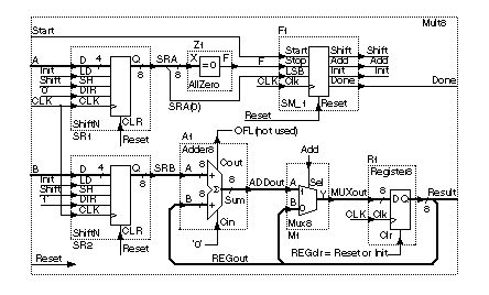
Table 10.9 shows
a schematic and the VHDL code that describes the interconnection of all
the components for the multiplier. Notice that the schematic comprises two
halves: an 8-bit-wide datapath section (consisting of the registers, adder,
multiplexer, and zero detector) and a control section (the finite-state
machine). The arrows in the schematic denote the inputs and outputs of each
component. As we shall see in Section 10.7, VHDL has strict rules about
the direction of connections.
TABLE 10.9 A
4-bit by 4-bit multiplier. |

|
entity Mult8 is
port (A, B: in BIT_VECTOR(3 downto 0); Start, CLK, Reset: in BIT;
Result: out BIT_VECTOR(7 downto 0); Done: out BIT); end Mult8;
architecture Structure of Mult8 is use work.Mult_Components.all;
signal SRA, SRB, ADDout, MUXout, REGout: BIT_VECTOR(7 downto 0);
signal Zero, Init, Shift, Add, Low: BIT := '0'; signal High: BIT := '1';
signal F, OFL, REGclr: BIT;
begin
REGclr <= Init or Reset; Result  <= REGout;
SR1 : ShiftN port map(CLK=>CLK,CLR=>Reset,LD=>Init,SH=>Shift,DIR=>Low ,D=>A,Q=>SRA);
SR2 : ShiftN port map(CLK=>CLK,CLR=>Reset,LD=>Init,SH=>Shift,DIR=>High,D=>B,Q=>SRB);
Z1 : AllZero port map(X=>SRA,F=>Zero);
A1 : Adder8  port map(A=>SRB,B=>REGout,Cin=>Low,Cout=>OFL,Sum=>ADDout);
M1 : Mux8    port map(A=>ADDout,B=>REGout,Sel=>Add,Y=>MUXout);
R1 : Register8 port map(D=>MUXout,Q=>REGout,Clk=>CLK,Clr=>REGclr);
F1 : SM_1    port map(Start,CLK,SRA(0),Zero,Reset,Init,Shift,Add,Done);
end;
|
10.2.7 Packages and Testbench
To complete and test
the multiplier design we need a few more items. First we need the following
"components list" for the items in Table 10.9:
package Mult_Components is
component Mux8 port (A,B:BIT_VECTOR(7 downto 0);
	Sel:BIT;Y:out BIT_VECTOR(7 downto 0));end component;
component AllZero port (X : BIT_VECTOR;
	F:out BIT );end component;
component Adder8 port (A,B:BIT_VECTOR(7 downto 0);Cin:BIT;
	Cout:out BIT;Sum:out BIT_VECTOR(7 downto 0));end component;
component Register8 port (D:BIT_VECTOR(7 downto 0);
	Clk,Clr:BIT; Q:out BIT_VECTOR(7 downto 0));end component;
component ShiftN port (CLK,CLR,LD,SH,DIR:BIT;D:BIT_VECTOR;
	Q:out BIT_VECTOR);end component;
component SM_1 port (Start,CLK,LSB,Stop,Reset:BIT;
	Init,Shift,Add,Done:out BIT);end component;
end;
Next we need some utility
code to help test the multiplier. The following VHDL generates a clock with
programmable "high" time ( HT ) and "low"
time ( LT ):
package Clock_Utils is
procedure Clock (signal C: out Bit; HT, LT:TIME);
end Clock_Utils;
package body Clock_Utils is
procedure Clock (signal C: out Bit; HT, LT:TIME) is
begin
	loop C<='1' after LT, '0' after LT + HT; wait for LT + HT;
	end loop;
end;
end Clock_Utils;
Finally, the following code
defines two functions that we shall also use for testing--the functions
convert an array of bits to a number and vice versa:
package Utils is
	function Convert (N,L: NATURAL) return BIT_VECTOR;
	function Convert (B: BIT_VECTOR) return NATURAL;
end Utils;
package body Utils is
	function Convert (N,L: NATURAL) return BIT_VECTOR is
		variable T:BIT_VECTOR(L-1 downto 0);
		variable V:NATURAL:= N;
		begin for i in T'RIGHT to T'LEFT loop
			T(i) := BIT'VAL(V mod 2); V:= V/2;
		end loop; return T;
	end;
	function Convert (B: BIT_VECTOR) return NATURAL is
		variable T:BIT_VECTOR(B'LENGTH-1 downto 0) := B;
		variable V:NATURAL:= 0;
		begin for i in T'RIGHT to T'LEFT loop
			if T(i) = '1' then V:= V + (2**i); end if;
			end loop; return V;
		end;
end Utils;
The following code tests the
multiplier model. This is a testbench (this simple example is not a comprehensive
test). First we reset the logic (line 17) and then apply a series of values
to the inputs, A and B . The clock generator (line
14) supplies a clock with a 20 ns period. The inputs are changed 1 ns after
a positive clock edge, and remain stable for 20 ns through the next positive
clock edge.
entity Test_Mult8_1 is end; -- runs forever, use break!!
architecture Structure of Test_Mult8_1 is
use Work.Utils.all; use Work.Clock_Utils.all;
	component Mult8 port
		(A, B : BIT_VECTOR(3 downto 0); Start, CLK, Reset : BIT;
		Result : out BIT_VECTOR(7 downto 0); Done : out BIT);
	end component;
signal A, B : BIT_VECTOR(3 downto 0);
signal Start, Done : BIT := '0';
signal CLK, Reset : BIT;
signal Result : BIT_VECTOR(7 downto 0);
signal DA, DB, DR : INTEGER range 0 to 255;
begin
C: Clock(CLK, 10 ns, 10 ns);
UUT: Mult8 port map (A, B, Start, CLK, Reset, Result, Done);
DR <= Convert(Result);
Reset  <= '1', '0' after 1 ns;
process begin
	for i in 1 to 3 loop for j in 4 to 7 loop
		DA <= i; DB <= j;
		A<=Convert(i,A'Length);B<=Convert(j,B'Length);
		wait until CLK'EVENT and CLK='1'; wait for 1 ns;
		Start <= '1', '0' after 20 ns; wait until Done = '1';
		wait until CLK'EVENT and CLK='1';
	end loop; end loop;
	for i in 0 to 1 loop for j in 0 to 15 loop
		DA <= i; DB <= j;
		A<=Convert(i,A'Length);B<=Convert(j,B'Length);
		wait until CLK'EVENT and CLK='1'; wait for 1 ns;
		Start <= '1', '0' after 20 ns; wait until Done = '1';
		wait until CLK'EVENT and CLK='1';
	end loop; end loop;
	wait;
end process;
end;
Here is the signal trace output
from the Compass Scout simulator:
      Time(fs) + Cycle            da           db           dr
----------------------  ------------ ------------ ------------
                  0+ 0:            0            0            0
                  0+ 1: *          1 *          4 *          0
...
           92000000+ 3:            1            4 *          4
...
          150000000+ 1: *          1 *          5            4
...
          193000000+ 3:            1            5 *          0
...
          252000000+ 3:            1            5 *          5
...
          310000000+ 1: *          1 *          6            5
...
          353000000+ 3:            1            6 *          0
...
          412000000+ 3:            1            6 *          6
Positive clock edges occur
at 10, 30, 50, 70, 90, ... ns. You can see that the output (dr)
changes from '0' to '4' at 92 ns, after five clock
edges (with a 2 ns delay due to the output register, R1).
Chapter start Previous page Next page
|


