|
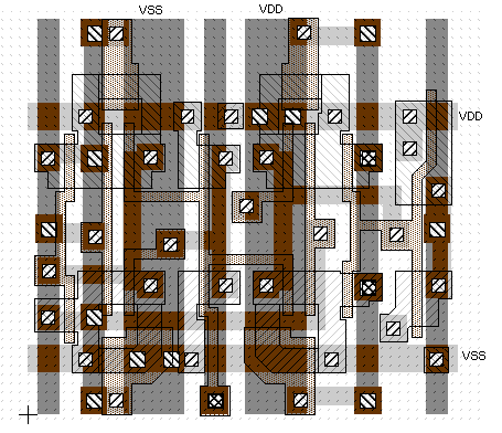
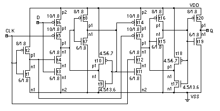
[ Chapter start ] [ Previous page ] [ Next page ] 3.8 Datapath-Cell DesignFigure 3.21 shows a datapath flip-flop. The primary, thicker, power buses run vertically on m2 with thinner, internal power running horizontally on m1. The control signals (clock in this case) run vertically through the cell on m2. The control signals that are common to the cells above and below are connected directly in m2. The other signals (data, q, and qbar in this example) are brought out to the wiring channel between the rows of datapath cells. Figure 3.22 is the schematic for Figure 3.21 . This flip-flop uses a pair of cross-coupled inverters for storage in both the master and slave latches. This leads to a smaller and potentially faster layout than the flip-flop circuits that we use in gate-array and standard-cell ASIC libraries. The device sizes of the inverters in the data-path flip-flops are adjusted so that the state of the latches may be changed. Normally using this type of circuit is dangerous in an uncontrolled environment. However, because the datapath structure is regular and known, the parasitic capacitances that affect the operation of the logic cell are also known. This is another advantage of the datapath structure.
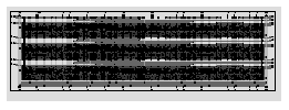
Figure 3.23 shows an example of a datapath. Figure 3.23 (a) depicts a two-level metal version showing the space between rows or slices of the datapath. In this case there are many connections to be brought out to the right of the datapath, and this causes the routing channel to be larger than normal and thus easily seen. Figure 3.23 (b) shows a three-level metal version of the same datapath. In this case more of the routing is completed over the top of the datapath slices, reducing the size of the routing channel.
[ Chapter start ] [ Previous page ] [ Next page ] | |||||||


