1.2 Design Flow
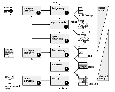
Figure 1.10 shows the sequence of steps to design an ASIC; we call this a
design flow
. The steps are listed below (numbered to correspond to the labels in Figure 1.10) with a brief description of the function of each step.
|

|
|
FIGURE 1.10 ASIC design flow.
|
-
Design entry.
Enter the design into an ASIC design system, either using a
hardware description language
(
HDL
) or
schematic entry
.
-
Logic synthesis.
Use an HDL (VHDL or Verilog) and a logic synthesis tool to produce a
netlist
—a description of the logic cells and their connections.
-
System partitioning.
Divide a large system into ASIC-sized pieces.
-
Prelayout simulation.
Check to see if the design functions correctly.
-
Floorplanning.
Arrange the blocks of the netlist on the chip.
-
Placement.
Decide the locations of cells in a block.
-
Routing.
Make the connections between cells and blocks.
-
Extraction.
Determine the resistance and capacitance of the interconnect.
-
Postlayout simulation.
Check to see the design still works with the added loads of the interconnect.
Steps 1–4 are part of
logical design
, and steps 5–9 are part of
physical design
. There is some overlap. For example, system partitioning might be considered as either logical or physical design. To put it another way, when we are performing system partitioning we have to consider both logical and physical factors. Chapters 9–14 of this book is largely about logical design and Chapters 15–17 largely about physical design.
|


