Details were disclosed at the company’s 3rd Annual US Samsung Foundry Forum
SANTA CLARA, Calif. — (BUSINESS WIRE) — May 22, 2018 — Samsung Electronics Co., Ltd., a world leader in advanced semiconductor technology solutions, today unveiled a series of new silicon innovations at the heart of future high-performance computing and connected devices.
This press release features multimedia. View the full release here: https://www.businesswire.com/news/home/20180522006421/en/
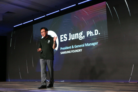
ES Jung, President and General Manager, at the 3rd Annual U.S. Samsung Foundry Forum in Santa Clara, CA (Photo: Business Wire)
With comprehensive process technology roadmap updates down to 3-nanometer (nm) at the annual ‘Samsung Foundry Forum (SFF) 2018 USA’, Samsung Foundry is focused on providing customers with the tools necessary to design and manufacture powerful, yet energy-efficient system-on-chips (SoC) for a wide range of applications.
“The trend toward a smarter, connected world has the industry demanding more from silicon providers,” said Charlie Bae, executive vice president and head of the Foundry Sales & Marketing Team at Samsung Electronics. “To meet that demand, Samsung Foundry is powering innovation at the silicon level that will ultimately give people access to data, analysis and insight in new and previously unthought-of ways to make human lives better. It is imperative for us to accomplish the first-time silicon success for our customers’ next-generation chip designs.”
Process Technology Roadmap Updates
- 7LPP (7nm Low Power Plus): 7LPP, the first semiconductor process technology to use an EUV lithography solution, is scheduled to be ready for production in the second half of this year. Key IPs are under development, aiming to be completed by the first half of 2019.
- 5LPE (5nm Low Power Early): Through further smart innovation from 7LPP process, 5LPE will allow greater area scaling and ultra-low power benefits.
- 4LPE/LPP (4nm Low Power Early/Plus): The use of highly mature and verified FinFET technology will be extended to the 4nm process. As the last generation of FinFET, 4nm provides a smaller cell size, improved performance and faster ramp-up to the stable level of yield by adopting proven 5LPE, supporting easy migration.
- 3GAAE/GAAP (3nm Gate-All-Around Early/Plus): 3nm process nodes adopt GAA, the next-generation device architecture. To overcome the physical scaling and performance limitations of the FinFET architecture, Samsung is developing its unique GAA technology, MBCFETTM (Multi-Bridge-Channel FET) that uses a nano-sheet device. By enhancing the gate control, the performance of 3nm nodes will be significantly improved.
HPC (High-Performance Computing) Solutions
Samsung Foundry delivers the technology solutions to drive the latest hyper-scale datacenters and accelerate the growth of Artificial Intelligence (AI) and Machine Learning capability. From the latest 7LPP technology and beyond with its EUV capability, to the differentiated high-speed IPs such as 100Gbps+ SerDes on top of the innovative 2.5D/3D heterogeneous packaging, Samsung delivers the total platform solutions to greatly increase computing power and accelerate AI revolution.
Connected Device Solutions
From low-power microcontroller units (MCU) and next-generation connected devices, to the most sophisticated autonomous vehicles based on 5G and Vehicle to Everything (V2X) communication, Samsung Foundry offers full-featured turnkey platforms to enable compelling products. A broad technology portfolio from 28/18 FD-SOI with eMRAM and RF capability to advanced 10/8nm FinFET processes will enable a great end-user experience for connected devices.
Mr. Bae continued, "Over the past year, we have focused on strengthening our EUV process portfolio to provide each of our customers with the finest technologies. Applying GAA structure to our next generation process node will enable us to take the lead in opening a new smart, connected world, while also to reinforcing our technology leadership."
Details regarding Samsung Foundry can be found at www.samsungfoundry.com and www.linkedin.com/company/samsungfoundry.
About Samsung Electronics Co., Ltd.
Samsung inspires the world and shapes the future with transformative ideas and technologies. The company is redefining the worlds of TVs, smartphones, wearable devices, tablets, digital appliances, network systems, and memory, system LSI, foundry and LED solutions. For the latest news, please visit the Samsung Newsroom at http://news.samsung.com.
View source version on businesswire.com: https://www.businesswire.com/news/home/20180522006421/en/
Contact:
Samsung Semiconductor, Inc.
Lisa Warren-Plungy, 408-544-5377
Email Contact