


- First Product on New Lattice Nexus FPGA Platform
- Up to 75 Percent Lower Power Compared to Similar Class Competitive Devices
HILLSBORO, Ore. — (BUSINESS WIRE) — December 10, 2019 — Lattice Semiconductor Corporation (NASDAQ: LSCC), the low power programmable leader, today announced the first FPGA developed on its new Lattice Nexus™ FPGA platform, CrossLink-NX™. This new FPGA provides the low power, small form factor, reliability, and performance that developers need to create innovative embedded vision and AI solutions for communications, compute, industrial, automotive, and consumer systems.
This press release features multimedia. View the full release here: https://www.businesswire.com/news/home/20191210005349/en/
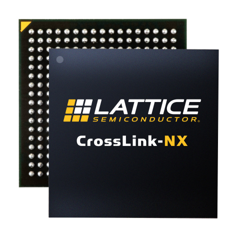
The new CrossLink-NX FPGA from Lattice Semiconductor (Graphic: Business Wire)
According to Patrick Moorhead, President and Founder of Moor Insights & Strategy, “Technology trends like 5G connectivity, cloud-based analytics, factory automation and the smart home are driving demand for embedded vision solutions that support machine learning. However, the data latency, cost and privacy issues associated with cloud-based ML analytics have sparked interest among developers in moving more data processing from the cloud to the Edge. But doing so requires OEMs have access to Edge AI/ML inferencing solutions that offer high performance data processing, low power operation, and a small form factor.”
FPGAs are a compelling hardware platform for embedded vision and AI applications, as they perform functions in parallel. This parallel architecture significantly accelerates certain processing workloads, including data inferencing.
“Embedded vision systems are growing in complexity; many systems today use multiple image sensors, displays and cameras. Implementing such systems at the Edge, where device size and power consumption are critical, adds even more design complexity,” said Bill Pu, Co-Founder and President, Leopard Imaging. “With their very low power consumption, small size, high-performance interfaces, and robust software and IP library, Lattice CrossLink-NX FPGAs let us quickly and easily develop different video signal bridging, aggregation and splitting applications for our industrial and automotive customers using just one device, saving us significant development time and resources.”
The CrossLink-NX family was designed using the new Lattice Nexus platform, which combines a 28 nm FD-SOI manufacturing process with a new, Lattice-designed, FPGA fabric architecture optimized for low power operation in a small form factor.
“Not only does CrossLink-NX lead in power consumption, form factor, reliability and performance in comparison to similar competing FPGAs, it is also supported by a robust library of design software, IP blocks and application reference designs,” said Gordon Hands, Director of Product Marketing, Lattice Semiconductor. “These make it quick and easy for developers to integrate CrossLink-NX FPGAs into new or existing Edge designs.”
Key features of the CrossLink-NX include:
- Low power – built on the Lattice Nexus FPGA platform, CrossLink-NX provides up to a 75 percent reduction in power consumption compared to competing FPGAs of a similar class.
- High reliability – CrossLink-NX has a Soft Error Rate (SER) up to 100 times lower than similar FPGAs in its class, making it a compelling solution for mission critical applications that must operate safely and reliably. The initial CrossLink-NX device is designed to support ruggedized environments found in outdoor, industrial, and automotive applications.
-
Performance – CrossLink-NX delivers enhanced performance enabled by three key elements:
- Fast I/O support – CrossLink-NX FPGAs are well-suited for embedded vision applications thanks to support for multiple fast I/Os, including MIPI, PCIe and DDR3 memory.
- Instant on performance – to better support applications where a long system boot time is unacceptable, such as industrial motor control, CrossLink-NX enables ultra-fast I/O configuration in 3 ms and total device configuration in less than 15 ms.
- High memory to logic ratio – to efficiently power AI inferencing in Edge devices, CrossLink-NX features 170 bits of memory for every logic cell, the highest memory to logic ratio in its class, providing 2x the performance compared to prior generations.
- Small form factor – to support customer system miniaturization, the first CrossLink-NX device is available in a 6 x 6 mm form factor which is up to ten times smaller than similar competing FPGAs in its class.
- Software tools and IP – in addition to its new Lattice Radiant 2.0 design software, Lattice offers a robust library of popular IP cores including interfaces like MIPI D-PHY, PCIe, SGMII and OpenLDI, and demos for common embedded vision applications such as 4:1 image sensor aggregation.
Originally scheduled for availability in 2020, Lattice is releasing CrossLink-NX ahead of schedule and is already sampling devices with select customers. For more information, please visit www.latticesemi.com/CrossLink-NX.
About Lattice Semiconductor
Lattice Semiconductor (NASDAQ: LSCC) is the low power programmable leader. We solve customer problems across the network, from the Edge to the Cloud, in the growing communications, computing, industrial, automotive and consumer markets. Our technology, long-standing relationships, and commitment to world-class support lets our customers quickly and easily unleash their innovation to create a smart, secure and connected world.
For more information about Lattice, please visit www.latticesemi.com. You can also follow us via LinkedIn, Twitter, Facebook, YouTube, WeChat, Weibo or Youku.
Lattice Semiconductor Corporation, Lattice Semiconductor (& design) and specific product designations are either registered trademarks or trademarks of Lattice Semiconductor Corporation or its subsidiaries in the United States and/or other countries. The use of the word “partner” does not imply a legal partnership between Lattice and any other entity.
GENERAL NOTICE: Other product names used in this publication are for identification purposes only and may be trademarks of their respective holders.
View source version on businesswire.com: https://www.businesswire.com/news/home/20191210005349/en/
Contact:
MEDIA CONTACTS:
Bob Nelson
Lattice Semiconductor
408-826-6339
Bob.Nelson@latticesemi.com
INVESTOR CONTACT:
Rick Muscha
Lattice Semiconductor
408-826-6000
Rick.Muscha@latticesemi.com


 Animation, 3D Art and 3D Models")