


Highest-Performing NAND Available; Cost-Effectively Reduces Latency
SAN JOSE, Calif. — (BUSINESS WIRE) — August 5, 2019 — Toshiba Memory America, Inc. (TMA), the U.S.-based subsidiary of Toshiba Memory Corporation, today announced the launch of a new Storage Class Memory (SCM) solution: XL-FLASH™. Based on the company’s innovative BiCS FLASH™ 3D flash memory technology with 1-bit-per-cell SLC, XL-FLASH brings low latency and high performance to data center and enterprise storage. Sample shipments will start in September, with mass production expected to begin in 2020.
This press release features multimedia. View the full release here: https://www.businesswire.com/news/home/20190805005229/en/
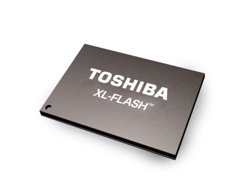
Based on Toshiba Memory's innovative BiCS FLASH™ 3D flash memory technology with 1-bit-per-cell SLC, XL-FLASH™ brings low latency and high performance to data center and enterprise storage. (Photo: Business Wire)
Classified as SCM (or persistent memory), with the ability to retain its contents like NAND flash memory, XL-FLASH bridges the performance gap that exists between DRAM and NAND. While volatile memory solutions such as DRAM provide the access speed needed by demanding applications, that performance comes at a high cost. As the cost-per-bit and scalability of DRAM levels off, this new SCM (or persistent memory) layer in the memory hierarchy addresses that issue with a high density, cost effective, non-volatile NAND flash memory solution. Poised for growth, industry analyst firm IDC estimates the SCM market is expected to reach in excess of $3B in 20221.
Sitting in between DRAM and NAND flash, XL-FLASH brings increased speed, reduced latency and higher storage capacities – at a lower cost than traditional DRAM. XL-FLASH will initially be deployed in an SSD format but could be expanded to memory channel attached devices that sit on the DRAM bus, such as future industry standard non-volatile dual in-line memory modules (NVDIMMs).
Key Features
- 128 gigabit (Gb) die (in a 2-die, 4-die, 8-die package)
- 4KB page size for more efficient operating system reads and writes
- 16-plane architecture for more efficient parallelism
- Fast page read and program times. XL-FLASH provides a low read latency of less than 5 microseconds, approximately 10 times faster than existing TLC2
As the inventor of NAND flash, the first to announce 3D flash memory technology and a leader in process migrations, Toshiba Memory is ideally positioned to deliver SLC-based SCM with mature manufacturing, proven scalability and time-tested SLC reliability.
“With XL-FLASH, we are giving hyperscalers and enterprise server/storage providers a more cost-effective, lower latency storage solution that bridges the gap between DRAM and NAND performance,” noted Scott Nelson, senior vice president and general manager of Toshiba Memory America, Inc.'s Memory Business Unit. “We’re also opening the door for emerging technologies and industry standards that will enable different form factors for low-latency flash memory solutions. SCM is the next frontier for enterprise storage, and our role as one of the world’s largest flash memory suppliers gives XL-FLASH a cost/performance edge over competing SCM solutions.”
For more information, please visit business.toshiba-memory.com.
About Toshiba Memory America, Inc.
Toshiba Memory America, Inc. is the U.S.-based subsidiary of Toshiba Memory Corporation, a leading worldwide supplier of flash memory and solid state drives (SSDs). From the invention of flash memory to today’s breakthrough 96-layer BiCS FLASH™ technology, Toshiba Memory continues to lead innovation and move the industry forward. For more information, please visit business.toshiba-memory.com and follow us on social media.
© 2019 Toshiba Memory America, Inc. All rights reserved. Information in this press release, including product pricing and specifications, content of services, and contact information is current and believed to be accurate on the date of the announcement, but is subject to change without prior notice. Technical and application information contained here is subject to the most recent applicable Toshiba Memory product specifications.
Notes:
[1] IDC May 2019 - Worldwide Solid State Drive Forecast, 2019-2023, Doc
# US43828819
[2] When compared to TMC’s TLC NAND which has a read
latency of approximately 50 microseconds.
Highest performing NAND available claim based on the fact that the die has been specifically designed (16 planes) to provide higher performance than TLC NAND.
All company names, product names and service names may be trademarks of their respective companies.
In every mention of a Toshiba Memory product: Product density is
identified based on the density of memory chip(s) within the Product,
not the amount of memory capacity available for data storage by the end
user. Consumer-usable capacity will be less due to overhead data areas,
formatting, bad blocks, and other constraints, and may also vary based
on the host device and application. For details, please refer to
applicable product specifications. The definition of 1Gb = 2^30 bits =
1,073,741,824 bits. The definition of 1GB = 2^30 bytes = 1,073,741,824
bytes. The definition of 1KB = 2^10 bytes = 1,024 bytes.


 Animation, 3D Art and 3D Models")